background image

ADJUSTMENT

Adjusting Idling Current
1. Preparation

(1)  Prepare a DV voltmeter.  
(2)   Place the unit in normal usage conditions, away from highly ventilated areas such as next to an air conditioning 

machine or electric fan.  
The set requires an ambient temperature of 15

~30

 and standard humidity.

(3)  Settings of This Unit
 

• POWER (Power source switch) 


STANDBY


• SPEAKER (Speaker terminal)  


No load


 ( Do not connect equipment such as speakers or dummy resistors. )

2.  Adjustment Procedure

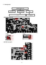
(1)   Remove the top cover and turn VR4800, VR4801, VR4802, VR4803, VR4804, VR4805, VR4806 of the AMP PCB as 

far anticlockwise(

c

) as possible.

(2)   Connect the DC Voltmeter test points.
 

FRONT-Lch  


 TP4800

 FRONT-Rch 


 TP4802


CENTER  ch  


 TP4804

 SURROUND-Lch  

 TP4806

  SURROUND-Rch  

 TP4808


SURROUND-BACK Lch 

 TP4801


SURROUND-BACK Rch 

 TP4813

(3)  Connect the power cord to an outlet. Next, press the power button to turn on the power.
(4)  Set this unit as follows.
 

MASTER VOLUME   

 "---" anticlockwise (

c

 min.)


SPEAKER (Speaker terminal) 

 No load


( Do not connect equipment such as speakers or dummy resistors. )

 MODE   


 MCH STEREO


FUNCTION  


 DVD

(5)   Turn VR4800 clockwise (

x

) and adjust the voltage of the test point to "

2.0mV ± 0.5mV DC

" within 2 minutes.

(6)  10 minutes after the preliminary adjustment, turn VR4800 and set the voltage as "

3.0mV ± 0.5mV DC

".

(7)  Adjust the variable resistance of each channel using the same method.

F Lch

S L ch

C ch

S R ch

F R ch

S Back Lch

S Back Rch

VR4803

TP4800

TP4806 VR4802

TP4804 VR4804

C

SR

SL

FL

VR4800

TP4808

TP4802

VR4801

VR4805

TP4810 VR4806

TP4813

SBR

SBL

FR

DC Voltmeter

AMP UNIT

73

Summary of Contents for NR1605/FB

Page 1: ...to the maximum extent possible Ver 2 Some illustrations using in this service manual are slightly different from the actual set Please use this service manual with referring to the operating instructions without fail For purposes of improvement specifications and design are subject to change without notice Please refer to the MODIFICATION NOTICE Service Manual ...

Page 2: ...rocessor etc 57 Firmware Update Procedure 57 1 Updating by USB 57 2 Updating by DPMS 66 ADJUSTMENT 73 SURROUND MODES AND PARAMETERS 74 TROUBLE SHOOTING 77 1 POWER 77 2 Analog video 78 3 HDMI DVI 82 4 AUDIO 84 5 Network Bluetooth USB 87 6 SMPS 92 CLOCK FLOW WAVE FORM IN DIGITAL BLOCK 94 LEVEL DIAGRAM 95 BLOCK DIAGRAM 101 POWER DIAGRAM 102 WIRING DIAGRAM 103 PRINTED Circuit BOARDS 104 SCHEMATIC DIAG...

Page 3: ... you can do with this manual Search for a Ref No phrase Ctrl Shift F You can use the search function in Acrobat Reader to search for a Ref No in schematic diagrams printed wiring circuit diagrams block diagrams and parts lists 1 Press Ctrl Shift F on the keyboard The Search window appears 2 Enter the Ref No you want to search for in the Search window and then click the Search button A list of sear...

Page 4: ...g Adobe Reader 9 On the Document menu click Sign Magnify schematic printed circuit board diagrams 1 Ctrl Space mouse operation Press Ctrl Space on the keyboard and drag the mouse to select the area you want to view The selected area is magnified When you want to move the area shown hold down Space and drag the mouse When you want to show a full page view press Ctrl 0 on the keyboard Ctrl Space 0 P...

Page 5: ...een Example using Adobe Reader 9 On the Tools menu point to Select Zoom and then click Pan Zoom Window Magnify schematic printed circuit board diagrams 3 Loupe Tool function The Loupe Tool function lets you magnify a specific part of a diagram in a separate window Example using Adobe Reader X On the View menu point to Zoom and then click Loupe Tool The Loupe Tool window appears on the screen Examp...

Page 6: ...tant safety parts that are indicated by the z mark on schematic diagrams and parts lists be sure to use the designated parts Be sure to mount parts and arrange the wires as they were originally placed For safety seasons some parts use tapes tubes or other insulating materials and some parts are mounted away from the surface of printed circuit boards Care is also taken with the positions of the wir...

Page 7: ... part make a clear distinction between 1 and I i to avoid mis supplying 3 A part ordered without specifying its part number can not be supplied 4 Part indicated by mark is not illustrated in the exploded view WARNING Parts indicated by the z mark have critical characteristics Use ONLY replacement parts recommended by the manufacturer INSTRUCTIONS FOR HANDLING SEMI CONDUCTORS AND OPTICAL UNIT Elect...

Page 8: ...Personal notes 8 ...

Page 9: ...eighted Direct mode Distortion MONO 0 7 1 kHz SRETEO 1 0 1 kHz n n Wireless LAN section Network type wireless LAN standard Conforming to Wi Fi z1 Security WEP 64 bit WEP 128 bit WPA WPA2 PSK AES WPA WPA2 PSK TKIP Radio frequency 2 4 GHz No of channels 1 11 ch for U 1 13 ch for N F z1 The Wi Fi CERTIFIED Logo and the Wi Fi CERTIFIED On Product Logo are registered trademarks of the Wi Fi Alliance n ...

Page 10: ...ns after confirming that the display flashes in intervals of approximately 1 second The unit is initialized NOTE If the status in step 3 does not occur start again from step 1 Initializing the device restores settings configured by the user to the factory settings Take note of your settings beforehand and reconfigure them after initialization Service Jigs The following jigs extension cable kit are...

Page 11: ...ADIATOR ASSY See DISASSEMBLY 2 RADIATOR ASSY and EXPLODED VIEW GUIDE CENTER FRONT PCB Ref No of EXPLODED VIEW 15 GUIDE CENTER PCB Ref No of EXPLODED VIEW 16 GUIDE PCB L Ref No of EXPLODED VIEW 18 AMP PCB Ref No of EXPLODED VIEW 24 GUIDE BT Ref No of EXPLODED VIEW 48 HDMI PCB See DISASSEMBLY 4 HDMI PCB and EXPLODED VIEW HDMI PCB ASSY Ref No of EXPLODED VIEW 47 CX870 MODULE ASSY Ref No of EXPLODED V...

Page 12: ...about the shooting direction of each photograph Photographs with no shooting direction indicated were taken from the top of the unit The photograph is NR1605U model The viewpoint of each photograph Shooting direction X View from the top Front side Shooting direction D Shooting direction C Shooting direction A Shooting direction B 12 ...

Page 13: ...SSY 1 Remove the screws 2 Cut the wire clamp then remove the connector wires and FFC Remove the Style pin and screws 3 Remove the screws View from the bottom Front side FFC FFC N7005 N7002 CP4401 CUT STYLE PIN Shooting direction D Shooting direction C 13 ...

Page 14: ...ng TOP COVER RADIATOR ASSY 1 Remove the screws 2 Remove the screws 3 Remove the connector wire and STYLE PIN 4 Remove the connector wire View from the bottom FFC FFC N7005 N7002 CP4401 STYLE PIN CP4800 CP4801 CP4803 CP4802 14 ...

Page 15: ... Remove the connector 4 HDMI PCB Proceeding TOP COVER HDMI PCB 1 Cut the wire clamp then remove the connector wires and FFC Remove the STYLE PIN 2 Remove the screws CP4604 CP4615 CP4614 Front side FFC FFC N7005 N7002 CON1 CON2 N1029 N1019 CP4142 CUT STYLE PIN CUT STYLE PIN 15 ...

Page 16: ...3 Remove the connector 5 AV PCB Proceeding TOP COVER HDMI PCB AV PCB 1 Remove the connector wire Remove the screws Front side N1033 N1018 N1014 N1015 N1013 N1016 Front side CP4002 CP4000 CP4615 CP4614 16 ...

Page 17: ...the connector wire and STYLE PIN Remove the PCB HOLDER and screws 7 POWER TRANS Proceeding TOP COVER HDMI PCB POWER TRANS 1 Remove the connector wire and STYLE PIN CP4001 STYLE PIN CP4800 CP4802 CP4803 STYLE PIN PCB HOLDER CP4001 STYLE PIN CP4604 STYLE PIN CP4142 17 ...

Page 18: ...t will separate and TRANS will fall from SET if screws is removed 8 SMPS PCB Proceeding TOP COVER SMPS PCB 1 Remove the connector wire Remove the screws See EXPLODED VIEW for instructions on how to remove each PCB of the SMPS PCB CP4401 STYLE PIN View from the bottom 18 ...

Page 19: ...taller Setup are not initialized M DAX ZONE2 SOURCE Initializes backup data Settings for the Installer Setup are not initialized 7 Factory Initialization mode Initialization includes settings for the Installer Setup ZONE2 SOURCE INTERNET RADIO Initializes backup data Initialization includes settings for the Installer Setup 8 Mode for preventing remote control acceptance M DAX DIMMER Start this uni...

Page 20: ...tion information w Firmware Package Version e Main µ com r Main 1st Boot Loader t DSP ROM y Audio PLD u Video PLD i GUI SFLASH o Ethernet 1st Boot Loader Hardware ID Q0 Ethernet 2nd Boot Loader Rhapsody Flag Q1 Ethernet IMAGE Q2 Ethernet MAC ADDRESS information Q3 BT MAC Address information q Model destination information FLD N R 1 6 0 5 U FLD N R 1 6 0 5 N FLD N R 1 6 0 5 K w Firmware Package Ver...

Page 21: ...apsody Flag FLD E t h e r n e t S B L Press the STATUS button FLD B 0 A Q1 Ethernet IMAGE FLD E t h e r n e t I M G Press the STATUS button FLD I Q2 Ethernet MAC ADDRESS information FLD N E T M A C A d d r e s s Press the STATUS button FLD Q3 BT MAC ADDRESS information FLD B T M A C A d d r e s s Press the STATUS button FLD 21 ...

Page 22: ...028 1029 is faulty In initial setting of i p Scaler ADV8003 there is not the reply of the Loopback Test result of the DDR memory I P S C A L E R E R R 0 2 r GUI Serial Flash NG In initial setting of i p Scaler ADV8003 there is not the reply of the Loopback Test result of the DDR memory G U I V E R E R R O R Check the firmware version t DIR NG This error is displayed if there is no re sponse from t...

Page 23: ...written in the Service Information GUI Image XXXX XXXX XXXX General Firmware Version Displays system information Main Sub 0 0 3 8 Info display 1 2 0 0 8 3 8 2 6 7 7 3 DSP X X 0 2 A PLD V PLD X X 0 1 X X 0 7 GUI X X X X 0 0 1 6 X X X 0 0 0 2 8 E FBL X X X X X X E SBL B X X X X X X X X X X X X E IMG I X X X X X X X X 0 0 3 7 The 1st digit from the right for DSP The 1st digit from the right for A PLD...

Page 24: ...hown on the display changes each time the button INTERNET RADIO is pressed Press the button STATUS to set the currently displayed mode and restart the device The On Off setting for each mode is shown by an asterisk b q FLD F P V O L L O C K O N The buttons on the unit and the master volume knob cannot be operated w FLD F P L O C K O N The buttons on the unit cannot be operated e FLD F P L O C K O ...

Page 25: ...ion shown on the display changes each time the button INTERNET RADIO is pressed Press the button STATUS to set the currently displayed mode and restart the device q FLD 1 S E R V I C E C H E C K Service Path Check Mode The Video and Audio paths can be checked This function is convenient for confirming problem paths in the product and executing a path check after repair w FLD 2 P R O T E C T I O N ...

Page 26: ...Personal notes 26 ...

Page 27: ...ck of Component input Component output Check of HDMI input IP Scaler HDMI output Check of ETHERNET input IP Scaler HDMI output The input source can be switched to any source except CBL SAT 2 HDMI pass MAIN ZONE V 0 3 H D M I P A S S Input Source CBL SAT Source of Video Convert IP Scaler OFF All sources MAIN ZONE ON ZONE2 OFF Check of HDMI input MAIN Function HDMI output MAIN The input source can b...

Page 28: ...er Config all Speaker Small SW Yes 2ch MAIN ZONE ON ZONE2 OFF Check the audio output Check of Analog input Speaker output Front L R Center Surround L R Surround Back L R Check of Analog input Pre OUT Front L R Subwoofer The input source can be switched to any source except CBL SAT Volume 20dB is the value when Relative settings are used The value is 60 when Absolute settings are used 6 Analog Amp ...

Page 29: ...24 COMP2 Cr COMP2 Cb COMP1 Cr COMP1 Cb VINB SW3 NJM2595MTE1 CVBS INPUT SW VIN2 VIN5 NJM2586AVC3 DVD MUTE SW2 VINB TMDS OUTPUT HDMI IN COMP2 Y COMP1 Y u COM CON IC CON VIN1 VIN3 VIN4 OUT PUT COMPONENT INPUT SW PCK 8bit Data VD0 VD7 CLK freg 27MHz BLU RAY CBL SAT MUTE OUT PUT SW1 VINC SW5 SW3 SW4 VINA TTL Data 480i_1080p Max 148 5MHz CLK freg TTL Data 480i_1080p Max 148 5MHz CLK freg DDRII OUT1 TMDS...

Page 30: ...COMP2 Cb COMP1 Cr COMP1 Cb VINB SW3 NJM2595MTE1 CVBS INPUT SW VIN2 VIN5 NJM2586AVC3 DVD MUTE SW2 VINB TMDS OUTPUT HDMI IN COMP2 Y COMP1 Y u COM CON IC CON VIN1 VIN3 VIN4 OUT PUT COMPONENT INPUT SW PCK 8bit Data VD0 VD7 CLK freg 27MHz BLU RAY CBL SAT MUTE OUT PUT SW1 VINC SW5 SW3 SW4 VINA TTL Data 480i_1080p Max 148 5MHz CLK freg TTL Data 480i_1080p Max 148 5MHz CLK freg DDRII OUT1 TMDS OUTPUT 4K 6...

Page 31: ...P2 Cb COMP1 Cr COMP1 Cb VINB SW3 NJM2595MTE1 CVBS INPUT SW VIN2 VIN5 NJM2586AVC3 DVD MUTE SW2 VINB TMDS OUTPUT HDMI IN COMP2 Y COMP1 Y u COM CON IC CON VIN1 VIN3 VIN4 OUT PUT COMPONENT INPUT SW PCK 8bit Data VD0 VD7 CLK freg 27MHz BLU RAY CBL SAT MUTE OUT PUT SW1 VINC SW5 SW3 SW4 VINA TTL Data 480i_1080p Max 148 5MHz CLK freg TTL Data 480i_1080p Max 148 5MHz CLK freg DDRII DDRII OUT1 TMDS OUTPUT 4...

Page 32: ...LK RXI2S3 DIRAMCKI RXI2S1 OPEN TC74VHCT244 TC74VHCT244 SLRCK TXSPDIF SPDIF Z2_DAC_DATA Z2_DAC_MCLK TMDS DAC_64FS DACDATAC DACDATASB TMDS DATAF DATAS TMDS 64FSDIR1 DATADIR1 NET USB_MCK NET USB_BCK DM920_SPDIF ARCSPDIF DIRADATAI MCLK PLDAERR DSP1OUTFS DSP1INSB SR DSP1INCSW C DSP1IN SW DSP1INFS DSP1INMCK TXSPDIF DIGITAL IN NET USB_LRCK HDMI2 0 Matix SW MN8647781 HDMI2 0 Matix SW MN8647781 DIRRXSPDIF ...

Page 33: ...L DSP_FR DSP_C ANA_FL Tone Tone Mix Bypass SBR SBL SL SR C FR FL ATT SW FL FM AM TUNER DVD TO PCM9211 1 6 F9 2ch PREOUT MIC Mini Jack SAT_CBL TO A PLD 1 6 I9 ZONE2 OUT 0 1ch PREOUT SPK OUT HEADPHONE OUT ANALOG INPUT ZONE2 VOLUME CONTROL FROM DIGITAL SBR FR B FR H BI AMP ZONE SBL FL B FL H BI AMP ZONE ZONE2 SB ASSIGN NR1605 ANALOG AUDIO DIAGRAM fig 04b 33 ...

Page 34: ...LK RXI2S3 DIRAMCKI RXI2S1 OPEN TC74VHCT244 TC74VHCT244 SLRCK TXSPDIF SPDIF Z2_DAC_DATA Z2_DAC_MCLK TMDS DAC_64FS DACDATAC DACDATASB TMDS DATAF DATAS TMDS 64FSDIR1 DATADIR1 NET USB_MCK NET USB_BCK DM920_SPDIF ARCSPDIF DIRADATAI MCLK PLDAERR DSP1OUTFS DSP1INSB SR DSP1INCSW C DSP1IN SW DSP1INFS DSP1INMCK TXSPDIF DIGITAL IN NET USB_LRCK HDMI2 0 Matix SW MN8647781 HDMI2 0 Matix SW MN8647781 DIRRXSPDIF ...

Page 35: ...COMP2 Cb COMP1 Cr COMP1 Cb VINB SW3 NJM2595MTE1 CVBS INPUT SW VIN2 VIN5 NJM2586AVC3 DVD MUTE SW2 VINB TMDS OUTPUT HDMI IN COMP2 Y COMP1 Y u COM CON IC CON VIN1 VIN3 VIN4 OUT PUT COMPONENT INPUT SW PCK 8bit Data VD0 VD7 CLK freg 27MHz BLU RAY CBL SAT MUTE OUT PUT SW1 VINC SW5 SW3 SW4 VINA TTL Data 480i_1080p Max 148 5MHz CLK freg TTL Data 480i_1080p Max 148 5MHz CLK freg DDRII OUT1 TMDS OUTPUT 4K 6...

Page 36: ...SL DSP_FR DSP_C ANA_FL Tone Tone Mix Bypass SBR SBL SL SR C FR FL ATT SW FL FM AM TUNER DVD TO PCM9211 1 6 F9 2ch PREOUT MIC Mini Jack SAT_CBL TO A PLD 1 6 I9 ZONE2 OUT 0 1ch PREOUT SPK OUT HEADPHONE OUT ANALOG INPUT ZONE2 VOLUME CONTROL FROM DIGITAL SBR FR B FR H BI AMP ZONE SBL FL B FL H BI AMP ZONE ZONE2 SB ASSIGN NR1605 ANALOG AUDIO DIAGRAM fig 07 36 ...

Page 37: ...LK RXI2S3 DIRAMCKI RXI2S1 OPEN TC74VHCT244 TC74VHCT244 SLRCK TXSPDIF SPDIF Z2_DAC_DATA Z2_DAC_MCLK TMDS DAC_64FS DACDATAC DACDATASB TMDS DATAF DATAS TMDS 64FSDIR1 DATADIR1 NET USB_MCK NET USB_BCK DM920_SPDIF ARCSPDIF DIRADATAI MCLK PLDAERR DSP1OUTFS DSP1INSB SR DSP1INCSW C DSP1IN SW DSP1INFS DSP1INMCK TXSPDIF DIGITAL IN NET USB_LRCK HDMI2 0 Matix SW MN8647781 HDMI2 0 Matix SW MN8647781 DIRRXSPDIF ...

Page 38: ...L DSP_FR DSP_C ANA_FL Tone Tone Mix Bypass SBR SBL SL SR C FR FL ATT SW FL FM AM TUNER DVD TO PCM9211 1 6 F9 2ch PREOUT MIC Mini Jack SAT_CBL TO A PLD 1 6 I9 ZONE2 OUT 0 1ch PREOUT SPK OUT HEADPHONE OUT ANALOG INPUT ZONE2 VOLUME CONTROL FROM DIGITAL SBR FR B FR H BI AMP ZONE SBL FL B FL H BI AMP ZONE ZONE2 SB ASSIGN NR1605 ANALOG AUDIO DIAGRAM fig 08b 38 ...

Page 39: ...LK RXI2S3 DIRAMCKI RXI2S1 OPEN TC74VHCT244 TC74VHCT244 SLRCK TXSPDIF SPDIF Z2_DAC_DATA Z2_DAC_MCLK TMDS DAC_64FS DACDATAC DACDATASB TMDS DATAF DATAS TMDS 64FSDIR1 DATADIR1 NET USB_MCK NET USB_BCK DM920_SPDIF ARCSPDIF DIRADATAI MCLK PLDAERR DSP1OUTFS DSP1INSB SR DSP1INCSW C DSP1IN SW DSP1INFS DSP1INMCK TXSPDIF DIGITAL IN NET USB_LRCK HDMI2 0 Matix SW MN8647781 HDMI2 0 Matix SW MN8647781 DIRRXSPDIF ...

Page 40: ...L DSP_FR DSP_C ANA_FL Tone Tone Mix Bypass SBR SBL SL SR C FR FL ATT SW FL FM AM TUNER DVD TO PCM9211 1 6 F9 2ch PREOUT MIC Mini Jack SAT_CBL TO A PLD 1 6 I9 ZONE2 OUT 0 1ch PREOUT SPK OUT HEADPHONE OUT ANALOG INPUT ZONE2 VOLUME CONTROL FROM DIGITAL SBR FR B FR H BI AMP ZONE SBL FL B FL H BI AMP ZONE ZONE2 SB ASSIGN NR1605 ANALOG AUDIO DIAGRAM fig 09b 40 ...

Page 41: ...LK RXI2S3 DIRAMCKI RXI2S1 OPEN TC74VHCT244 TC74VHCT244 SLRCK TXSPDIF SPDIF Z2_DAC_DATA Z2_DAC_MCLK TMDS DAC_64FS DACDATAC DACDATASB TMDS DATAF DATAS TMDS 64FSDIR1 DATADIR1 NET USB_MCK NET USB_BCK DM920_SPDIF ARCSPDIF DIRADATAI MCLK PLDAERR DSP1OUTFS DSP1INSB SR DSP1INCSW C DSP1IN SW DSP1INFS DSP1INMCK TXSPDIF DIGITAL IN NET USB_LRCK HDMI2 0 Matix SW MN8647781 HDMI2 0 Matix SW MN8647781 DIRRXSPDIF ...

Page 42: ...L DSP_FR DSP_C ANA_FL Tone Tone Mix Bypass SBR SBL SL SR C FR FL ATT SW FL FM AM TUNER DVD TO PCM9211 1 6 F9 2ch PREOUT MIC Mini Jack SAT_CBL TO A PLD 1 6 I9 ZONE2 OUT 0 1ch PREOUT SPK OUT HEADPHONE OUT ANALOG INPUT ZONE2 VOLUME CONTROL FROM DIGITAL SBR FR B FR H BI AMP ZONE SBL FL B FL H BI AMP ZONE ZONE2 SB ASSIGN NR1605 ANALOG AUDIO DIAGRAM fig 10b 42 ...

Page 43: ...LK RXI2S3 DIRAMCKI RXI2S1 OPEN TC74VHCT244 TC74VHCT244 SLRCK TXSPDIF SPDIF Z2_DAC_DATA Z2_DAC_MCLK TMDS DAC_64FS DACDATAC DACDATASB TMDS DATAF DATAS TMDS 64FSDIR1 DATADIR1 NET USB_MCK NET USB_BCK DM920_SPDIF ARCSPDIF DIRADATAI MCLK PLDAERR DSP1OUTFS DSP1INSB SR DSP1INCSW C DSP1IN SW DSP1INFS DSP1INMCK TXSPDIF DIGITAL IN NET USB_LRCK HDMI2 0 Matix SW MN8647781 HDMI2 0 Matix SW MN8647781 DIRRXSPDIF ...

Page 44: ...L DSP_FR DSP_C ANA_FL Tone Tone Mix Bypass SBR SBL SL SR C FR FL ATT SW FL FM AM TUNER DVD TO PCM9211 1 6 F9 2ch PREOUT MIC Mini Jack SAT_CBL TO A PLD 1 6 I9 ZONE2 OUT 0 1ch PREOUT SPK OUT HEADPHONE OUT ANALOG INPUT ZONE2 VOLUME CONTROL FROM DIGITAL SBR FR B FR H BI AMP ZONE SBL FL B FL H BI AMP ZONE ZONE2 SB ASSIGN NR1605 ANALOG AUDIO DIAGRAM fig 11b 44 ...

Page 45: ...SL DSP_FR DSP_C ANA_FL Tone Tone Mix Bypass SBR SBL SL SR C FR FL ATT SW FL FM AM TUNER DVD TO PCM9211 1 6 F9 2ch PREOUT MIC Mini Jack SAT_CBL TO A PLD 1 6 I9 ZONE2 OUT 0 1ch PREOUT SPK OUT HEADPHONE OUT ANALOG INPUT ZONE2 VOLUME CONTROL FROM DIGITAL SBR FR B FR H BI AMP ZONE SBL FL B FL H BI AMP ZONE ZONE2 SB ASSIGN NR1605 ANALOG AUDIO DIAGRAM fig 12 45 ...

Page 46: ...SL DSP_FR DSP_C ANA_FL Tone Tone Mix Bypass SBR SBL SL SR C FR FL ATT SW FL FM AM TUNER DVD TO PCM9211 1 6 F9 2ch PREOUT MIC Mini Jack SAT_CBL TO A PLD 1 6 I9 ZONE2 OUT 0 1ch PREOUT SPK OUT HEADPHONE OUT ANALOG INPUT ZONE2 VOLUME CONTROL FROM DIGITAL SBR FR B FR H BI AMP ZONE SBL FL B FL H BI AMP ZONE ZONE2 SB ASSIGN NR1605 ANALOG AUDIO DIAGRAM fig 13 46 ...

Page 47: ...LK RXI2S3 DIRAMCKI RXI2S1 OPEN TC74VHCT244 TC74VHCT244 SLRCK TXSPDIF SPDIF Z2_DAC_DATA Z2_DAC_MCLK TMDS DAC_64FS DACDATAC DACDATASB TMDS DATAF DATAS TMDS 64FSDIR1 DATADIR1 NET USB_MCK NET USB_BCK DM920_SPDIF ARCSPDIF DIRADATAI MCLK PLDAERR DSP1OUTFS DSP1INSB SR DSP1INCSW C DSP1IN SW DSP1INFS DSP1INMCK TXSPDIF DIGITAL IN NET USB_LRCK HDMI2 0 Matix SW MN8647781 HDMI2 0 Matix SW MN8647781 DIRRXSPDIF ...

Page 48: ...L DSP_FR DSP_C ANA_FL Tone Tone Mix Bypass SBR SBL SL SR C FR FL ATT SW FL FM AM TUNER DVD TO PCM9211 1 6 F9 2ch PREOUT MIC Mini Jack SAT_CBL TO A PLD 1 6 I9 ZONE2 OUT 0 1ch PREOUT SPK OUT HEADPHONE OUT ANALOG INPUT ZONE2 VOLUME CONTROL FROM DIGITAL SBR FR B FR H BI AMP ZONE SBL FL B FL H BI AMP ZONE ZONE2 SB ASSIGN NR1605 ANALOG AUDIO DIAGRAM fig 14b 48 ...

Page 49: ...een the speaker terminals or speakers with an impedance outside the rating were connected Abnormal DC output from the power amp Note Short circuits in speaker terminals or speakers can be identified If the power is turned on during this abnormality protection is activated after around 6 seconds and the power is turned off 4 THERMAL if the last protection was THERMAL A or THERMAL B or THERMAL E FLD...

Page 50: ... protection history is cleared FLD N O P R O T E C T 2 Initialize this unit See Initializing This Unit 10 page b Use the method in 3 5 3 1 if you do not want to erase your settings from this unit Warning Displays by POWER LED If the power is turned off while a protection is detected the POWER LED red flashes in the following ways as a warning according to the protection status 1 ASO DC protection ...

Page 51: ...IO and press the button STATUS to commit the selection 3 6 3 Operations Press the STATUS button after starting this device in Operation Info mode The following information is displayed in the following order a Accumulated operating time FLD O P T i m e H Time display STATUS b Power on count FLD P O n T i m e Count display STATUS c DC ASO Protection count FLD D C A S O STATUS d Thermal Protection c...

Page 52: ...ing the button INTERNET RADIO and press the button STATUS to commit the selection 3 7 3 Displays Start this unit in TUNER STEP mode select using button INTERNET RADIO and enter using button STATUS The following information is displayed in the following order a AM9kHz FM50kHz selected FLD A M 9 F M 5 0 INTERNET RADIO ZONE2 SOURCE b AM10KHz FM200kHz selected FLD A M 1 0 F M 2 0 0 STATUS C Press the ...

Page 53: ... returning to the normal display 5 CX870 CY920 Reboot mode 5 1 Actions The CX870 CY920 is restarted after CX870 CY920 hangup The CX870 CY920 can be restarted even in the network standby setting Setup menu Network Network Always On 5 2 Operations 1 Turn on the button MAIN ZONE and set NETWORK as the input source 2 Hold down buttons DIMMER and SOUND MODE for at least 3 seconds while the power is on ...

Page 54: ... Playback station 6 2 Operations Hold down buttons DIMMER and STATUS for at least 3 seconds while the power is on Initializing Display FLD I n i t i a l i z i n g FLD I n i t i a l i z i n g FLD I n i t i a l i z i n g FLD I n i t i a l i z i n g Complete Display FLD C o m p l e t e d This is displayed for 5 seconds before returning to the normal display Failed Display FLD F a i l e d 54 ...

Page 55: ...ary CAUTION Incorrect connections may cause malfunction Connection of Jig for HDMI PCB Items to Be Prepared 8U 110084S EXTENSION UNIT KIT 1 Set Insulation sheet Not supplied 1 sheet Ground lead Not supplied 1 pc Procedures 1 Remove the screws 2 Remove the connector PCB Front side N1033 N1018 N1014 N1015 N1013 N1016 HDMI PCB 55 ...

Page 56: ...onnect the expansion cables Connection table of Board to Board No Pin Ref No PCB Ref No PCB q 23pin CP4603 SIDE CNT N1014 HDMI w 15pin CP4604 SIDE CNT N1015 HDMI e 7pin CP4605 SIDE CNT N1013 HDMI r 23pin CP4606 SIDE CNT N1016 HDMI t 17pin CP4613 FRONT CNT N1018 HDMI y 11pin CP4612 FRONT CNT N1013 HDMI HDMI PCB Insulation sheet CHASSIS HDMI CONNECTOR FRONT_CNT PCB SIDE_CNT PCB HDMI PCB 1 2 3 4 5 6 ...

Page 57: ...eeds to be written after replacement See Firmware Update Procedure for information on writing the software D The software has been written Be sure to rewrite with the latest software for your service region See Firmware Update Procedure for information on writing the software FIRMWARE UPDATE PROCEDURE 1 Updating by USB The latest firmware can be downloaded to a USB memory for updates 1 1 Connectin...

Page 58: ... ID NR1605U North America U 100100240100 NR1605N Europe N 100100240200 NR1605F Japan F 100100240400 firmwares 000100XXXXXX APLD bin DSP bin enc_update xml GUI bin IMG bcd MAIN bin SBL bcd SUB bin VPLD bin 1 4 Insert the USB memory in the USB port NOTE Remove the LAN cable from this unit when performing updates Download firmware in USB flash drive 58 ...

Page 59: ...e the USB memory before the update is finished Never turn off the power before an update is completed It takes around 1 hour to complete the update Once an update is started normal operations cannot be performed until it is completed The GUI menu settings and image adjustment settings of this unit may be initialized Take note of your settings beforehand and reconfigure them after the update 1 9 Fo...

Page 60: ...o n n e c t i o n F a i l 0 9 This unit automatically retries several times Wait until the FL display stops If the FL display stops at the Error dis play press and hold the Power opera tion button for five seconds 0A Unable to detect USB for Firm ware Download C o n n e c t i o n F a i l 0 A Disconnect and connect the USB mem ory 0B No Firmware File for Firmware Download F i l e s N o t F o u n d ...

Page 61: ...led to obtain entire Firmware information after SBL Mode C o n n e c t i o n F a i l 2 3 Disconnect and connect the USB mem ory 24 Time Out while obtaining entire Firmware information after SBL Mode C o n n e c t i o n F a i l 2 4 This unit automatically retries several times Wait until the FL display stops If the FL display stops at the Error dis play press and hold the Power opera tion button fo...

Page 62: ... until the FL display stops If the FL display stops at the Error dis play press and hold the Power opera tion button for five seconds 50 Unable to detect USB C o n n e c t i o n F a i l 5 0 This unit automatically retries several times Wait until the FL display stops If the FL display stops at the Error dis play press and hold the Power opera tion button for five seconds 51 No Firmware File in USB...

Page 63: ...s several times Wait until the FL display stops If the FL display stops at the Error dis play press and hold the Power opera tion button for five seconds 61 Mismatched Check Sum in re sponse or no response from Sub for I command U p d a t e C h e c k N G 6 1 This unit automatically retries several times Wait until the FL display stops If the FL display stops at the Error dis play press and hold th...

Page 64: ... Wait until the FL display stops If the FL display stops at the Error dis play press and hold the Power opera tion button for five seconds A6 Error notification received while requesting Firmware Info U p d a t i n g f a i l A 6 This unit automatically retries several times Wait until the FL display stops If the FL display stops at the Error dis play press and hold the Power opera tion button for ...

Page 65: ...re version after updating After updating the firmware check the version See 1 Version Display Mode 20 page 1 11 Device display during firmware update Display of target device during firmware update Target device Display Error code when an error occurs Main CPU M a i n m i n 08 0B 10 15 20 27 36 3B 3F Sub S u b m i n 50 52 54 58 5A 64 Audio PLD A P L D m i n 50 52 54 58 5A 64 VIDEO PLD V P L D m i ...

Page 66: ...display disappears during the update The remaining time of the update is shown on the display of the unit The normal status resumes after the update is completed Precautions for Updates The environment and settings must allow connection to broadband Internet for updates Never turn off the power before an update is completed It takes around 1 hour to complete the update Once an update is started no...

Page 67: ...re there is a small network load 08 Error notification received while requesting Firmware Info C o n n e c t i o n F a i l 0 8 Check the network connection Update in an environment where there is a small network load 09 Time Out while obtaining Firm ware information C o n n e c t i o n F a i l 0 9 Check the network connection Update in an environment where there is a small network load 0A Error NG...

Page 68: ...ct notification SBL Mode after DPMS connection L o g i n f a i l e d 2 2 Initialize the unit and try updating again Update in an environment where there is a small network load 23 Server congestion notification SBL Mode after DPMS connection S e r v e r i s b u s y 2 3 Update in an environment where there is a small network load 24 Connection failure notification SBL Mode after DPMS connection C o...

Page 69: ...onnection L o g i n f a i l e d 5 0 Update in an environment where there is a small network load 51 Server congestion notification by DPMS connection S e r v e r i s b u s y 5 1 Update in an environment where there is a small network load 52 Connection failure notification DPMS connection C o n n e c t i o n F a i l 5 2 Check the network connection Update in an environment where there is a small n...

Page 70: ...start up Sub in Power On sequence during Update U p d a t i n g f a i l 6 2 Turn on the power again Update will start automatically 80 Write Enable Latch Bit not set in Read after issuing WREN com mand U p d a t i n g f a i l 8 0 Turn on the power again Update will start automatically 81 Block Erase failed in Read after issuing BE command U p d a t i n g f a i l 8 1 Turn on the power again Update ...

Page 71: ...n load D o w n l o a d f a i l A E Turn on the power again Update will start automatically Update in an environment where there is a small network load AF Error ServerBusy notification re ceived while requesting Firmware Download D o w n l o a d f a i l A F Turn on the power again Update will start automatically Update in an environment where there is a small network load B0 Error Connect failure ...

Page 72: ...P L D m i n 50 52 54 58 5A 61 VIDEO PLD V P L D m i n 50 52 54 58 5A 64 DSP D S P m i n 50 52 54 58 5A 61 GUI Serial Flash G U I m i n 50 52 54 58 5A 61 80 86 CX870 Boot Loader E S B L m i n A0 A4 A6 A7 AE B5 CX870 Image E I M G m i n A0 A4 A6 A7 AE B5 CX870 Image Emergency Mode U p d a t e r e t r y Checking the Firmware Version After an Update After updating the firmware check the version See 1 ...

Page 73: ...ch TP4802 CENTER ch TP4804 SURROUND Lch TP4806 SURROUND Rch TP4808 SURROUND BACK Lch TP4801 SURROUND BACK Rch TP4813 3 Connect the power cord to an outlet Next press the power button to turn on the power 4 Set this unit as follows MASTER VOLUME anticlockwise c min SPEAKER Speaker terminal No load Do not connect equipment such as speakers or dummy resistors MODE MCH STEREO FUNCTION DVD 5 Turn VR480...

Page 74: ... channel s There are two playback modes Cinema mode that is optimized for movie playback Music mode that is optimized for music playback DTS Surround This mode can be selected when playing sources recorded in DTS DTS ES Dscrt6 1z This mode is suitable for playing discs recorded in DTS ES The surround back channel added using the discrete method is played as an independent channel Since all channel...

Page 75: ... PLg gx Music z2 S Dolby PLg gx Game z2 S Dolby PLg gz z2 S S S DTS Neo 6 Cinema z2 S DTS Neo 6 Music z2 S Multi Ch Stereo S S S Virtual S S S z1 2 channel also includes analog input z2 This mode plays back 2 channel sources in 5 1 or 7 1 channel playback It cannot be selected when headphones are used or when the speaker configuration is front speakers only Contents Connections Playback Settings T...

Page 76: ... In 7 1 S S S Multi In Dolby EX S S S Multi In PLgx Cinema S Multi In PLgx Music S Multi In PLgz S S S Multi channel z3 Multi Ch Stereo S S S Virtual S S S z3 The sound mode that can be selected differs depending on the audio format of the input signal and the number of channels For details see Types of input signals and corresponding sound modes v p 245 Contents Connections Playback Settings Tips...

Page 77: ...any faulty parts TO 3 5 Protection History Display Mode See 49 page Are any parts not fully con nected in the connectors that connect the PCBs Is DC5V output even when the connector N1029 supplying power from the SMPS PCB to the HDMI PCB is removed Check the circuits around the Microprocessor on the HDMI PCB and replace any faulty parts Check for breakages and short circuits in the circuits and pa...

Page 78: ... R1943 R1944 R1969 R1968 C2091 R1967 C2090 C1181 U1006 BD82065FVJ E2 C1430 N1027 R1576 R1934 R1597 R1594 R1573 R1001 SW1 C1201 C1202 N1011 R1792 C1774 R1785 C1738 R1226 R1520 N1025 R1481 R1518 R1517 R1515 C1509 C1357 R1483 R1513 R1254 D1030 D1029 D1023 D1022 D1020 D1021 C2104 R1993 C1078 Q1043 N1035 R1763 R1766 R1824 R1821 N1033 C1686 L1059 C1688 R1737 U1061 C1689 C1690 C1691 Q1010 U1002 SN74CBT32...

Page 79: ...onfirmed at the following points HDMI PCB V R2092 COMPONENT Y R2089 COMPONENT Cb R2091 COMPONENT Cr R2090 Check the connection between the PCBs Input CVBS Check B Input COPONENT Check C Output CVBS NG Check B 4 Output COMPONENT NG Check C 4 Output HDMI NG See 3 HDMI DVI NO NO YES q 79 ...

Page 80: ... from the video amplifier CVBS IC5401 1pin The circuit between IC5401 and JK5400 are faulty Check the IC5401 power supply voltage and check the soldering of the surrounding circuits The circuit between IC5401 and JK5400 are faulty Use the jigs to extend the HDMI PCB The HDMI PCB is faulty Check the connection between the FRONT CONNECTOR PCB and the VIDEO PCB NO NO NO YES YES YES b All parts are VI...

Page 81: ...COMP CR IC5402 16pin The circuit between IC5402 and JK5402 are faulty Use the jigs to extend the HDMI PCB The HDMI PCB is faulty Check the connection between the FRONT CONNECTOR PCB and the AV PCB NO NO NO YES YES YES b All parts are VIDEO PCB parts unless otherwise specified w q e r Check the IC5402 power supply voltage and check the soldering of the surround ing circuits The circuit between IC54...

Page 82: ... of the fluorescent display lit Proceed to YES if using a Blu ray DVD player from another compa ny 9 Is sound output from the speaker terminal of this unit when the power of the TV is turned off or the cable connecting the TV to this unit is removed Check the connection of the HDMI DVI cable Use a certified HDMI cable with the HDMI mark Replace the HDMI DVI cable with one shorter than 5m 2m is rec...

Page 83: ...ports HDCP Computer monitors can not be used Check the instruction manual of the TV and check the input setting The TV is faulty Check the circuits around the IP SCALER U1026 HDMI PCB and DDR2 U1028 1029 If there appear to be no problems U1026 or U1028 1029 is faulty If the TV does not support 1080P a picture cannot be output even if the Blu ray DVD player is set to 1080P NO NO NO YES NO See NR160...

Page 84: ...M or DolbyDigital or dts CHECK4 INPUT SURROND MODE SOURCE Audio output OK HDMI Don t care Legacy PCM2ch or DolbyDigital or dts CHECK6 INPUT Connect AVR s connected in HDMI audio out put OK HDMI This unit s HDMI OUT Other AVR s HDMI IN Setting SURROND MODE SOURCE CEC STANDBY Don t care HBR audio DolbyTrueHD or dtsHD MA CHECK5 INPUT SURROND MODE SOURCE Audio output OK HDMI Don t care HBR audio Dolby...

Page 85: ...immer potentiometer between the base of the power transistor open 1kΩ Are any other transistors faulty Are any other resistors faulty Turn on the power and check that the voltage of each part is correct and that there is an idling current Replace the power transistor Replace the transistor Replace the resistor Replace the emitter resistor Replace the base resistor Replace the trimmer potentiometer...

Page 86: ...io signal in AV PCB CN4801 Is electron volume serial data being sent to AV PCB CP5200 Once more connect the connectors correctly If the malfunctioning channel and function can be identified check the corresponding signal path Repair the 7V power supply Repair the power amplifier Is the connector correctly connected with HDMI PCB YES NO YES NO YES NO 86 ...

Page 87: ...ces have the same IP address and that the subnet mask settings are correct Connect the peripheral devices correctly Check the instruction manual of the router and configure the settings correctly Check that there are no connection restric tions by MAC addresses etc NO NO NO 5 Network Bluetooth USB 5 1 Cannot connect to the network Is the LAN cable correctly inserted Insert the LAN cable correctly ...

Page 88: ...R1 U1018 uCOM 53pin Hi Is E_POWER4 U1018 uCOM 53pin Hi Is E_POWER2 U1018 uCOM 54pin Hi The circuit of D5V_POWER between U1018 and U1070 are faulty The circuit of E_POWER1 between U1018 and Q1071 are faulty The circuit of E_POWER4 between U1018 and Q1071 are faulty The circuit of E_POWER2 between U1018 and U1069 are faulty The circuit around U1070 DC DC Conv is faulty The circuit around Q1071 FET_S...

Page 89: ...PCB Can a waveform 32 768kHz be confirmed pin 4 of IC6000 on Blue tooth PCB Is 1pin LDO_ON of Bluetooth PCB CP6001 Hi The circuit between the AC inlet and N1036 is faulty Check the SMPS PCB The circuit between N1036 of the HDMI PCB and CP6001 of the Bluetooth PCB are faulty of wire or board The circuit around Q1071 or U1070 of the HDMI PCB is faulty The circuit around U6001 is faulty The oscillati...

Page 90: ...rmed between pin 1 and pin 4 of CP4402 USB Connector on USB PCB The USB signal circuit between CX870 and CP4402 of the USB PCB are faulty Check the AUDIO circuit of U1024 DSP or later Are CN4401 of the 870 JUNCTION PCB and N7000 of the USB PCB correctly connected Are I2S signal output to pin 26 28 30 34 of the U1008 HDMI PCB The 30 32 34pin in the case of DSD Are audio signal output to pin 8 of U1...

Page 91: ... DATA 5 2V 5 2V GND GND 7 BT_RX GND CLAMP7000 BKT7001 BD82065FVJ E2 1 BT_ACTIVE 4 BT_LDO_ON 3 WLAN_ACTIVE 5 BT_PRIORITY 11 GND 10 5V BKT7000 120PIN PLUG 2 BT_EINT N7005 CX870 JUNCTION PCB 7020 07500 020 0S N7000 U7000 35 30 25 45 40 30 50 5 15 H PR 16 H PGND 17 H PL NET2 5V NET1 8V NET1 2V 10 RLY_HIB 11 H P_RLY 12 SB_RLY 3 V_INC 5 V_INA 4 V_INB 50 60 40 90 80 100 A 12MHZ 9 DGND 11 DGND 7 DGND 2 VA...

Page 92: ... the soldering of the PCB Check the damage of each part Replace the damaged part s Replace the damaged part s Has a fuse F4140 broken Are there any short circuits caused by the soldering of the PCB Are any parts damaged Replace the IC4140 TOP258MG and D4142 D4143 D4144 D4145 DC 5V is not output YES YES YES YES YES YES 6 SMPS 92 ...

Page 93: ...PTION OPTION Ü Ü Ü Ü After primary side rectification Caution High voltage electric shock Primary drain Caution High voltage electric shock After secondary rectifications A B C Operation waveform for each part A B C A B C SMPS unit Unloaded Set 93 ...

Page 94: ...148 R2152 R2157 R2179 R2180 R1674 R1673 R1682 R1677 R1676 C1161 C1160 D1073 C1752 R1783 L1117 R1985 D1115 R1396 R1398 R1399 C1845 C1698 L1136 C1948 C2164 C2119 C2134 C2129 C2136 C2111 C2168 C2128 C2125 R1356 R1374 C1293 R1249 C1907 C2087 D1136 D1137 R1956 R1959 R1958 C1203 C1204 R1222 R1244 R1243 C1172 R1241 R1238 R1237 R1220 R1270 R1271 R1449 R1463 R1464 C1708 R1363 R1742 D1104 U1033 R1908 R1906 ...

Page 95: ...MAX SIGNAL LEVEL DOLBY LIMIT LEVEL ALLch 3dBFS GAIN setting of MASTER VOL 00dB SW YES DIGITAL 2 0dB 2 0dB SW YES ANALOG 2 0dB 6 5dB 4 5dB SW NONE DIGITAL 2 0dB 12dB 10 0dB SW NONE ANALOG 2 0dB 12dB 6 5dB 16 5dB 1 2 3 1 Basic OFFSET of VOL 0dB 2 OFFSET of SW NON 3 OFFSET of the AD input 2 12 10 0dB 2 12 6 5 16 5dB 3dB SW NO 32dBFS DIG IN 38 5dBFS A D IN 20dBFS DIG IN 26 5dBFS A D IN LINE IN EXT IN ...

Page 96: ...GRAM CENTER ch 2dB 0dBFS 10dBFS 20dBFS 30dBFS 40dBFS 20dBFS DIG IN PCM or DD Config1 26 5dBFS A D IN 200mV 30dB SP OUT 4 48Vrms 8Ω 29dB MAX SIGNAL LEVEL DOLBY LIMIT LEVEL ALLch 3dBFS 3dB 26 5dBFS DIG IN DD Config2 2 6 5 4 5dB EXT IN SPEAKER DSP R2A15218FP GAIN SR5009 ONLY PCM1690 D A PLD PRE OUT MUTE SR5009 ONLY 96 ...

Page 97: ...h 2dB 0dBFS 10dBFS 20dBFS 30dBFS 40dBFS 200mV 30dB MAX SIGNAL LEVEL 9 5dB 2 20 6 12dB Config1 DOLBY LIMIT LEVEL ALLch 3dBFS 50dBFS 40dBFS DIG IN DD Config1 INPUT 30dBFS DD LFE PREOUT 317mVrms 34dBFS PCM IN 40 5dBFS A D IN INPUT 20dBFS DIG IN PCM 200mV A D IN EXT IN DSP R2A15218FP GAIN PRE OUT MUTE SR5009 ONLY PCM1690 D A PLD PRE OUT MUTE SW1 97 ...

Page 98: ...10dBFS 20dBFS 30dBFS 40dBFS 23dBFS DIG IN PCM or DD Config1 29dBFS A D IN 200mV 30dB SP OUT 4 48Vrms 8Ω 29dB 2 6 4dB MAX SIGNAL LEVE Config2 DOLBY LIMIT LEVEL 1 41Vrms ALLch 3dBFS 6dB 29 5dBFS DIG IN DD Config2 2 6 5 4 5dB EXT IN SPEAKER DSP R2A15218FP GAIN SR5009 ONLY PCM1690 D A PLD PRE OUT MUTE SR5009 ONLY PREOUT 150mVrms 98 ...

Page 99: ...8Ω 26dB 2 3 6 7dB NON CLICP MAX SIGNAL LEVEL 4 0Vrms Config2 DOLBY LIMIT LEVEL 1 41Vrms ALLch 3dBFS 3dB 26dBFS DIG IN DD EX Config1 2 3 1dB DOLBY LIMIT LEVEL 1 41Vrms ALLch 3dBFS SP OUT D A OUT 32 5dBFS DIG IN DD EX Config2 INPUT 23dBFS DIG IN D D 2 6 5 3 7 5dB INPUT 200mV A D IN Mch STEREO EXT IN SPEAKER DSP R2A15218FP GAIN SR5009 ONLY PCM1690 D A PLD PRE OUT MUTE SR5009 ONLY PREOUT 150mVrms 99 ...

Page 100: ... 30dB 40dB 10dB LINE IN 0dBFS 2 0Vrms PREOUT 18 0dB 0dBFS 10dBFS 20dBFS 30dBFS 40dBFS 20dBFS DIG IN PCM5100 200mV MAX SIGNAL LEVEL 2 00Vrms SPEAKER 30dB SP OUT D A from DA SB ch TO MAIN from F ch NET USB DAC R2A15218FP ZONE2 BD3812F LEVEL DIAGRAM ZONE2 16 0dB 100 ...

Page 101: ...GND SL GND FRONT R GND ADV7850 HDMI TX HDMI RX DIR ADC MAIN_CPU SUB_CPU 40P SHIELD CARD CABLE DGND BD3812F SMPS_S3 SPK B D FRONT_CNT B D HDMI B D PLATE NJM2595M NJM2586A R2A15218FP MAIN TRANS AMP B S1 HDMI RX OPT COAX SIDE_CNT B D AV B D REG B D FRONT B D 7CH AMP B D SMPS B D AC CORD CURRENT DETECT VOLTAGE DETECT REG_CNT B D BLOCK DIAGRAM 101 ...

Page 102: ...OPEN S5 VKK S1 AMP B AC CORD S6 FILAMENT S2 8V 8V S4 VIDEO MAIN TRANS MAIN PWR ON DA3 3V NET1 9V NET1 9V NET1 9V CX870 NET1 8V CX870 OPEN NET1 2V CX870 NET3 3V CX870 MF1341S2164 POWER DIAGRAM 102 ...

Page 103: ...CX870 7P 8P 5P PLATE PLATE 2P 7P 4P 7P 11P 5P 8P PLATE S30SC6MT WIRING DIAGRAM 103 ...

Page 104: ...MO 5 DM920L 6 DAGND 7 DM920R 8 DACRTNGND 9 DACRTNGND 10 VAUXL 11 SW 8 CEN 10 SW 16 RC_IN 15 MUTE3 3V 14 REMOTE3 3V 17 FRONT_IRIN 18 RC_OUT 14 MIC 12 VAUXR 13 MICGND 15 VOL_MUTE 17 SR 14 SL 16 SR 19 KILLIR_MZ 22 ZVOL_CLK 23 ZVOL_DATA 21 ZVOL_LATCH 54 14 FRONT_RLY 8 AMPSIG_DET 9 THERMALDETC 2 COMP_SW2 6 COMP_SW1 70 8 DECIN_CB 10 DECIN_CR 4 DECIN_V A CEC1 1V1 D3 3V2 D5 2V 1 TU_SCLK SCL 4TU_RST ST 2 T...

Page 105: ...5208 R5300 Q5204 C5281 R5355 D5218 D5225 R5335 C5521 R5534 R5264 C 5 2 5 6 R5333 Q5217 R5441 D5227 R5548 R5345 11 SBL 13 SBR 9 FR 7 SR 5 C 1 FL 8 RLY_F 9 H P_R 11 H P_L 4 AGND 5 A 7V 3 A 7V 1 H PR 2 H PGND 5 RLY_SB 4 RLY_H P 3 H PL 9 RL B 8 RLY_HIB 7 RLY_F CR CR CB CB 3 SL 13 RLGND 1 THERMALDETC 6 A 7V 7 AGND 9 M DGND 10 TU_ 5V 3 A 7V 4 A 7V 18 AGND 12 AGND 6 AGND 9 A D_R 10 DAGND 11 A D_L 8 DAGND...

Page 106: ...061 RLY4004 CN4000 JACK4000 J4122 J4114 J4022 AC AC D4006 RLY4001 JACK4001 SBR NC AC_L CEN AC_H AC_H NC AC_L HIGHB HIGHB HIGHB HIGHB HIGHGND HIGHGND NC FR SL CEN FL H PL H PGND H PR RLY_H P RLY_SB RL B RLY_F HIB_RLY RLGND MUTE 7V M DGND SBLGND PREGND SR BONDING BONDING RLY_S C CLP4002 SBL CLP4009 F4100 A 7V CURRENT_DET THERMALDET A 7V CLP4001 F4000 AMPSIGDET AGND SPK B D T6 3AL 250V CLP4000 T6 3AL...

Page 107: ... AMP B D 7028 07481 101 0 SBL Q4801 R4815 C4804 R4952 R4964 R4911 R4923 R4993 R4985 C4873 R4863 R5032 R5030 R5026 D4800 C4811 C4801 R4950 R4915 R4907 R4903 R4873 C4866 R4986 C4826 D4810 D4809 R5034 D4829 D4830 R5046 R5027 R5071 R4892 D4812 D4805 D4827 D4835 R4891 R4828 R4820 R4818 R4811 R4832 R4948 D4817 R4944 R4945 D4820 D4819 Q4821 Q4839 R4991 R5001 R4989 R4868 D4825 Q4812 R4875 R4879 R5042 Q484...

Page 108: ...6 3V D4147 J4149 ZD4147 ZD4148 D4148 R4153 C4155 C4152 ZD4150 ZJ22B R4159 Pb R4140 IN OP FI ADJ ICT RLY4140 J4153 ZD4154 ZJ22B C4143 0 1UF 275V L4140 CN4141 J4146 C4168 C4164 5600UF 6 3V C4169 C 4 1 5 3 J4150 PC123 IC4142 BAR CODE J4142 J4144 ZD4153 ZJ22B D4141 R4164 R4149 D4145 D4140 R4143 ZD4160 CP4142 ZD4155 ZJ22B BKT4141 BURRING C4142 C4141 R4150 D4142 ZD4151 ZJ22B D4143 C4149 C4148 C4151 ZD41...

Page 109: ...70 47K R1071 D1006 OPEN D1008 OPEN D1009 OPEN D1010 OPEN D1011 OPEN 10K R1039 47K R1040 C1005 1N K C1006 1N K 10K R1014 47K R1015 RX2_5V 10P 1608 C1078 C1079 100N K C1080 100N K R1060 47 R1062 47 C1017 100N K C1086 1N K C1081 100N K C1020 100N K C1022 100N K R1059 47 C1084 100N K C1024 100N K C1025 100N K C1036 OPEN C1037 OPEN C1048 OPEN C1050 OPEN C1051 OPEN C1033 OPEN C1039 OPEN C1041 OPEN C1053...

Page 110: ...110 OPEN C1112 OPEN C1118 4 7U K 1608 C1126 4 7U K 1608 C1140 4 7U K 1608 C1151 4 7U K 1608 C1098 4 7U K 1608 C1114 4 7U K 1608 C1147 OPEN C1149 OPEN RX7_2 RX7_1 RX7_2 RX7_1 RX7_0 C1152 100N K RX7_C RX6_2 RX6_1 RX6_0 C1141 100N K RX6_C C1128 100N K RX7_DDCCL RX6_DDCCL RX5_DDCCL RX4_DDCCL RX7_5V P3_DDCDA P2_DDCDA R1165 1K8 R1160 1K8 P3_D1 P3_D2 C1156 1U 1608 P3_D0 P3_D0 C1145 1U 1608 R1145 510 D 16...

Page 111: ... FLASH_DOUT FLASH_CLK 10K R1252 OPEN R1251 0 R1240 0 R1250 ETH_RX ETH_RX ETH_TX R1264 33 R1242 100 NET USB_BCK R1238 100 NET USB_MCK R1236 100 DM920_SPDIF R1235 0 SPF1 RTC3V3 C1188 100N K EXT_FLASH_CS DEBUG_TX DEBUG_RX NET USB_DATAF FL NET USB_BCK NET USB_MCK NET USB_LRCK R1215 10K OPEN FLASH_DOUT SPI_DOUT RXD0 EXT_FLASH_CS 1N K C1201 100N K C1202 FLASH_WPROT USBOTG_VBUS MII_TX_CLK USB_OTG_DP HUB_...

Page 112: ...COMPONENT Y BT_EINT WLAN_ACTIVE BT_PRIORITY BT_RX BT_TX L6002 0 BT_3 3V BT_ACTIVE L6001 CB05YTYH221 LDO_ON CLK_32K L6000 CB05YTYH221 X6000 32 768KHz FC 135 NR1605 BT Mother B D CP6001 TO N7005 112 1 2 3 4 5 6 7 8 9 10 11 12 13 14 15 16 A B C D E F G H J K L M A B C D E F G H J K L M 1 2 3 4 5 6 7 8 9 10 11 12 13 14 15 16 ...

Page 113: ...IB RC_OUT KEY2 FIL_CTRL R1369 33K C1286 100N K C1287 100N K KEY1 C1289 10N K R1370 18K DC_PROT SB_RLY THERMALDETC OPEN M3 3V C1291 OPEN R1352 OPEN THER_PROTB ASO_PROT R1373 OPEN R1355 16K MIC_DET C1293 10N K R1356 100 THERMALDETB R1375 OPEN R1359 120K C1295 10N K R1360 100 ASODET R1377 OPEN R1363 120K C1297 10N K R1364 100 MIC_DET DGND SWM3 3V C1298 100N K TXD_MO232I CURRENT_DET DIRECT_LED ZVOL_CL...

Page 114: ...GND DAGND DAGND DAC_SR DAC_SL DAGND DAC_C DAC_FR DAGND FLRST GRN_LED H P_DET FL_DATA FIL_CTRL DIRECT_LED ZVOL_DATA ZVOL_LATCH M3 3V FL5V R1384 OPEN KEY2 L1029 0 2012 L1027 0 2012 ZVOL_CLK RC_IN WAKE_UP RC_OUT VOL_DATA H PL VAUXV MIC VAUXL VAUXR TU_SDIO SDA TU_RST ST PRE_Z2_MUTE D5V DA 7V DA 7V DA 5V VSELA D MGND ISELA KEY2 MICDET FL DATA H PL POWERKEY FRONT_IRIN MIC VAUXV VAUXL VAUXR A 7V A 7V D M...

Page 115: ...Q RESET BDOWN E_POWER3 E_POWER1 IR FLASHER OPTION_A NR1605N F OPEN Ø OPTION TABLE C1343 OPEN OPEN C1345 Q1037 RT1P141C BIR BM1341W D1095 OPEN C1341 NR1605U OPEN Ø OPTION TABLE DGND CURRENT_DET 100N K C1330 100N K C1332 KEY1 R1421 0 CPU_POWER THER_PROTB C1325 100N K FL_DATA M DAX_LED R1403 33 R1404 33 R1406 33 R1407 33 E_SPI_CS HUB_CONTROL R1400 0 E_FACT_RST HUB_SDA R1386 OPEN 3 4 2 1 12MHz FA 238V...

Page 116: ..._RST1 DAC_MC DAC_MS1 SUB_TDO AP_DA C1355 8P J HPD2 HPD4 HPD6 AP_CK C1356 8P J HPD8 AVSCL SCPUTXD R1514 33 R1497 33 CLKSIMO SOMI R1489 2M2 R1494 4K7 CEC_OUT 220K R1498 C1347 OPEN R1485 10K R1487 100K C1348 100N K CEC_COM SCPU3 3V SCPUTXD DGND MD NC NC CEC_COM HINSELC HINSELA HSDA SW1_RST HPD3 HPD1 HAINT0 C1352 100N K SUB_TDI R1472 33 HSDA SW2_RST C1353 100N K R1474 33 HPD6 778_3 778_2 HPD4 TX_RST D...

Page 117: ... 10N K 0 2012 L1036 0 2012 L1035 DDC_SCL TX_EN CEC RX_2 DGND RX_1 RX_0 RX_0 RX_C DGND CEC3 3V CEC5V DDCA_SCL TX_EN CEC 10K R1558 Q1046 RT1N141C 10U K 2012 C1391 1 3 4 2 R1665 0 2 AR 1 3 4 2 R1657 0 2 AR 1 3 4 2 R1663 0 2 AR DDC_SDA C1381 OPEN 0 2012 L1034 HPA_D RX_2 RX_1 DGND DGND DGND RX_C DGND CEC3 3V HDMI5V DDCA_SDA HPDF 19 17 15 13 11 9 8 7 6 5 4 3 2 18 16 14 12 10 1 HD 19F SMT 028 19P W O N10...

Page 118: ... 32 28 17 18 19 20 21 22 23 24 25 26 27 U1023 W9864G6JH 6 VDDQ DQ0 VDD VSSQ DQ2 DQ1 DQ3 VSSQ DQ4 VDDQ DQ5 DQ6 VSSQ DQ7 VDD LDQM WE VSS DQ8 VDDQ DQ9 DQ10 VSSQ DQ11 DQ12 VDDQ DQ13 DQ14 UDQM NC A8 A9 A11 CKE CLK A4 A5 A6 A7 VSS CAS RAS CS BA0 BA1 A10 AP A0 A1 A2 A3 VDD VSS DQ15 A12 1 0 16 7PB 2 N1035 GND EMU0 TMS TDO TCK DSP1RST DSP1FLAG0 OPEN R1576 C1479 100N K C1471 1N K 47 R1594 C1462 100N K C1460...

Page 119: ...49 CB05YTYH221 C1552 100N K C1553 10N K MISO DV3 3V DGND J20 J22 H22 L22 K22 TX1_2 TX1_1 TX1_0 TX1_C TX1_2 TX1_1 TX1_0 TX1_C DR_TXDQSB0 DR_TXDQSB1 47 R1694 R1696 47 4 AR R1698 47 4 AR DR_TXDQS2 R1700 47 4 AR 47 R1701 R1703 47 4 AR R1705 47 4 AR R1707 47 4 AR DR_TXRASB DR_TXCASB 47 R1688 R1710 47 4 AR 47 R1711 TX_DDRVREF 47 R1689 DDR_1 8V OPEN C1601 ADV8003_SPI_CS ADV8003_SPI_MO R1683 10K R1631 1K8...

Page 120: ...2 DR_TXDQ14 DDR_1 8V DGND DDR2 DDR2 DR_TXDQS2 DR_TXDQSB2 DDR2 DDR2 DDR2 DR_TXDM3 DR_TXDQ20 DR_TXDQ22 DR_TXDQ24 DR_TXDQ26 DDR_1 8V DDR2 DDR2 DR_TXDQ28 DR_TXDQ30 DGND DDR1 DDR1 DDR1 DDR1 DDR1 DDR1 DDR1 DDR2 DDR2 OPEN R1719 DDR2 DR_TXA2 DR_TXCKE DR_TXA0 DR_TXA1 OPEN R1721 OPEN R1724 OPEN R1726 DDR2 DDR2 DDR2 DDR2 DR_TXA3 DR_TXA4 DR_TXA5 DR_TXA6 OPEN R1728 OPEN R1730 DDR2 DDR2 100N K C1671 C1672 1U K ...

Page 121: ...C1959 OPEN C1693 1U K 1608 C1856 OPEN C1857 OPEN C1858 OPEN C1859 OPEN C1861 OPEN C1926 OPEN C1965 OPEN C1698 2 2U K 1608 C1863 OPEN C1866 OPEN C1970 OPEN D1106 OPEN R1817 3K3 RT1N141C Q1060 100N K C1681 C1868 OPEN C1869 OPEN C1967 OPEN C1872 OPEN C1873 OPEN C1875 OPEN D1104 LBAS16HT1G C1708 15N K 1608 C1674 OPEN D1105 LBAS16HT1G 470 6 3 MVG C1675 C1676 OPEN R1748 100 C1678 100N K 470 6 3 MVG C168...

Page 122: ...03_DDCSCL CEC_COM L1085 CB05YTYH221 L1083 CB05YTYH221 C2055 CH 10P C2038 100N K C2030 100N K C2026 100N K C2025 100N K 10 R1867 10K R1868 10 R1864 10 R1858 P1TX1_DDCSCL P0TX0_DDCSCL P0TX0_DDCSDA 108 142 P1TX1_DDCSDA P1TX1_0 P1TX1_0 P1TX1_2 P1TX1_2 P0TX0_0 P0TX0_0 P0TX0_1 P0TX0_1 P0TX0_C P0TX0_C P0TX0_DDCSDA P1TX1_HPD P0TX0_HPD R1880 0 R1876 0 0 R1877 R1873 0 R1859 OPEN OPEN R1860 TXC SHIELD ADV800...

Page 123: ...TS 0 0047UF 680 Ø OPEN R1969 100N K C2090 OPEN R1963 C2086 100N K FSDIR1 256FSDIR1 DIR_DIN C2078 100N K DATAS DATAF TXSPDIF TX64FS DV_POWER1 RXI2S1 RXI2S3 RX64FS 100N K C2069 100N K C2066 33 R1942 33 R1931 SUB_TMS SUB_TCK SUB_TDO DACDATASB DACDATAC DAC64FS DIRRXSPDIF DGND DV3 3V DGND Z2_DAC_MUTE Z2_DAC_BCLK Z2_DAC_DATA OPT2 OPT1 COAX1 1 2 RCA 107C BK K1003 COAX2 OPEN C2075 OPEN R1919 0 1608 A DIN_...

Page 124: ...Y10 R6 PO8KI_Y8 R4 PO8KI_Y6 R2 PO8KI_Y4 R0 PO8KI_Y2 G6 PO8KI_Y3 G7 PO8KI_Y1 G5 PO8KI_C11 G3 PO8KI_C9 G1 PO8KI_C7 B7 PO8KI_C5 B5 PO8KI_C3 B3 PO8KI_C1 B1 8KOPI_C0 B0 8KOPI_C2 B2 8KOPI_C4 B4 8KOPI_C6 B6 8KOPI_C8 G0 8KOPI_C10 G2 8KOPI_Y0 G4 8KOPI_Y2 G6 8KOPI_Y4 R0 8KOPI_Y3 G7 8KOPI_Y5 R1 8KOPI_Y7 R3 8KOPI_Y9 R5 8KOPI_Y11 R7 8KOPI_PCK 8KOPI_HSYNC PO8KI_HSYNC PO8KI_DE PO8KI_Y10 R6 PO8KI_Y8 R4 PO8KI_Y6 R...

Page 125: ...0 1608 R2021 100 1608 R2013 100 1608 R2002 100 1608 SBR SBR SR SR CEN CEN FR FR DM920R DM920L DAGND SBL SR SBR DAGND SW CEN DAGND FR FL DAGND A DIN_L A DIN_R 100N K C2174 100N K C2168 R2053 OPEN 100N K C2110 1N K C2112 C2179 2 2U M C2169 100N K 1N K C2114 1N K C2116 1N K C2118 1N K C2120 R2057 0 10K R2061 1N K C2122 1N K C2124 1N K C2126 1N K C2127 1N K C2129 1N K C2131 1N K C2133 1N K C2135 100N ...

Page 126: ... C2280 100N K C2302 100N K C2240 100N K C2242 100N K C2282 100N K C2283 10N K C2244 10N K C2246 10N K C2248 100N K C2250 10N K C2285 10N K C2287 10N K C2288 10N K C2289 10N K C2290 100N K C2303 10N K C2304 4 7U K 1608 C2305 10N K C2252 100N K C2254 4 7U K 1608 C2255 10N K C2293 4 7U K 1608 C2309 DDCB_SCL SPDIF DSD0A HPD_P2 P2_DDCDA P2_D2 P2_D1 P2_D0 P2_C P2_C RX_COM_5V RX_COM_5V P1_DDCDA P1_D2 P1_...

Page 127: ... VBUS R7019 OPEN R7018 OPEN 870VS 870PCK 870VD7 870VD5 870VD2 870VD1 OPEN R7024 USB_PWR_EN USBOTG_VBUS 10K R7021 USB_OTG_DN USB_OTG_DP AV3CTRL0 10K R7016 E_SPI_REQ I2C_SCL E_FACT_RST R7027 0 E_SPI_CS E_SPI_MIEO R7038 0 10UF 6 3V 2012 C7007 HDMI GND ETH_RX ETH_TX ETH_TX NET USB_DATAF FL NET USB_BCK NET USB_MCK CX870_SPDIF DEBUG_TX OPEN 2012 C7012 OPEN R7046 OPEN R7044 R7040 OPEN GND L7001 CB05YTYH2...

Page 128: ... PRE_MUTE 3P_JACK SBR SBL FR SL FL SR R5355 47 C5281 100N K DAGND USB_R MIC_IN FRONT IRIN ZVOL_LATCH C5282 100N K R5353 4K7 D5229 LBAS16HT1G Q5222 RT1P141C R5350 OPEN R5351 OPEN Q5223 RT1P141C 100 R5348 R5349 100 RT1P141C Q5220 R5354 18K IC5200 R2A15218FP F8 TO 8F CN5202 TO CP4002 CN5201 TO CP4000 CN4801 TO CP4801 CP5200 TO CN4604 CP5201 TO CN4602 CP5202 TO CN4606 CN5200 TO CP4614 F7 TO 7F 128 1 2...

Page 129: ...C VINB H IN3 SW2 H L H L H H SW2 SW4 SW3 NJM2595MTE1 DVD DVD H L MUTE SW5 H L u COM CON H H H IN2 OUT PUT L H L IC CON L H H L H L CVBS INPUT SW CBL SAT NR1605 L MUTE H H BLU RAY CBL SAT OUT PUT NJM2586AVC3 SW1 MUTE PS INPUT COMPONENT INPUT SW CN5402 TO CP4611 129 1 2 3 4 5 6 7 8 9 10 11 12 13 14 15 16 A B C D E F G H J K L M A B C D E F G H J K L M 1 2 3 4 5 6 7 8 9 10 11 12 13 14 15 16 ...

Page 130: ...P J 1608 R5572 820 1608 N1B N1SG KST MW104MV1 S63G 11K 1608 R5570 OPEN 1608 R5553 11K 1608 R5561 R5552 16K 1608 OPEN 1608 R5544 C5525 CH 240P J 1608 R5535 300K 1608 C5533 CH 330P J 1608 11K 1608 R5528 R5531 11K 1608 OPEN 1608 R5559 C5535 100 16 MVG KST MW004MV1 S63SV 1 KST MW004MV1 S63 1 C5526 CH 1500P J 1608 R5583 OPEN 1608 C5522 CH 1500P J 1608 C5520 CH 1500P J 1608 R5563 OPEN 1608 C5516 CH 1500...

Page 131: ...G AUDIO DIGITAL AUDIO TMDS SIGNAL VIDEO SIGNAL COMPONENT Y F9 TO 9F G0 TO 0G CP4801 TO CN4801 CN4800 TO N1019 CP4802 TO CN4005 CP4800 TO CN4000 131 1 2 3 4 5 6 7 8 9 10 11 12 13 14 15 16 A B C D E F G H J K L M A B C D E F G H J K L M 1 2 3 4 5 6 7 8 9 10 11 12 13 14 15 16 ...

Page 132: ...WER LINE POWER LINE ANALOG AUDIO DIGITAL AUDIO TMDS SIGNAL VIDEO SIGNAL COMPONENT Y 9F TO F9 0G TO G0 CP4803 TO CN4003 132 1 2 3 4 5 6 7 8 9 10 11 12 13 14 15 16 A B C D E F G H J K L M A B C D E F G H J K L M 1 2 3 4 5 6 7 8 9 10 11 12 13 14 15 16 ...

Page 133: ... M 50V R4002 10 1 5 L4002 SP 2507 R4001 10 1 5 L4000 SP 2507 1 0 3216 R4059 R4055 0 3216 C4019 2N2 K C4016 2N2 K C4061 100N K C4060 100N K C4062 100 16 RT1N237C Q4000 RT1N237C Q4002 3 2 1 RT1N237C Q4006 100N K C4058 R4042 100 10 50V C4059 VOLTAGE DETECT 10 2 R4013 C4013 47N M 50V R4005 10 1 5 R4006 10 1 5 R4011 10 2 C4004 47N M 50V C4012 47N M 50V L4005 SP 2507 C4003 47N M 50V R4010 10 2 L4003 SP ...

Page 134: ...A_ 7V A_ 7V M DGND 232IMO RC_OUT RC_IN R4641 4K7 2SA2166 Q4606 232IMO M DGND Z2_MUTE PRE_MUTE DA_FL DA_FL DAGND DAGND DA_C DA_FR DA_FR DA_SW DAGND DA_SW DA_SL DA_SR DAGND DA_SL DA_SR DAGND DAGND DA_SBR DA_SBL DA_SBR DA_SBL A D_L A D_R DAGND DAGND RETGND RETGND MICGND MIC_IN TU_SEN TU_SCLK SCL RC_IN RC_OUT TU_GPIO2 TUNED ZVOL_CLK D5V RC 5 MVOL_CLK D5V RC 5 REMOTE3 3V ZVOL_CLK R4642 4K7 N4600 1 0 11...

Page 135: ...MICGND H PL H PR MICDET 560 R4453 BD4401 0 BD4400 0 C4449 1 50 3 5 100 R4456 2K2 R4454 BD4402 CB05YTYH221 D4415 LBAS16HT1G C4452 100N K H P MIC 100 R4401 EC16B24T01D4ZZZ C4410 OPEN C4418 1 50 R4421 100 100 R4422 Q4402 RT1N141C USB_YS UA 002 13 CP4402 ZJ5 1B ZD4406 C4448 100N K R4455 100K C4446 10 16 3 5 R4444 0 EC16B24S0 ZZZ 100P J C4425 100P J C4426 D4407 OPEN 100P J C4427 7 4 5 6 2 3 1 8 CP4403 ...

Page 136: ...FB ZJ39B ZJ5 1B ZD4147 ZD4160 ZJ39B ZJ39B ZD4149 OPTION 2M2 5 R4149 270K R4147 OPTION 100 200 OPEN C4149 C4151 1N4007 D4147 OPTION BKT4142 MAINPOWER DGND D5 2V Ü Ü CHASSIS GND BKT4141 L4140 T6 3AL T6 3AL NR1605 F4141 F4141 OPEN OPEN 2M2 5 ZJ39B OPTION OPTION OPEN OPEN 1M 5 NR1605 27mH Ø LINE_FILTER OPTION Ø FUSE OPTION 2M2 5 ZJ39B ZD4148 R4148 Ø OPTION TABLE OPEN 1M 5 R4150 C4148 Ü Ü Ü Ü Ü Ü NR160...

Page 137: ...621 1N4007 C4613 100N M 50V F4604B F4603B AC_IN AC_IN 3 1 2 IC4600 KIA7805API D4634 OPEN 100 16 C4605 1SS133 D4607 OPEN ZD4601 D4608 OPEN 100N M 50V C4612 C4615 OPEN OPEN C4614 8V_IN AGND AGND AGND 8V_IN 5V_IN VGND 5V_IN F4603A D4617 1N4007 D4616 1N4007 1N4007 D4625 D4624 1N4007 JP4630 JUMPER 1 2 3 4 CN4607 120MM 4P C4602 10 50 D4600 1SS133 2 3 1 IC4608 KIA7812API D4611 OPEN 1 3 2 IC4603 KIA7908PI...

Page 138: ...TC 1 2 3 4 CP4615 20010WR 04 VIDEO 5V VIDEO_GND VIDEO_GND VIDEO 5V SMPS_REG_FCNT 3 3 CP4611 TO CN5402 CP4615 TO CN4607 CP4612 TO N1033 CP4614 TO CN5200 CP4613 TO N1018 138 1 2 3 4 5 6 7 8 9 10 11 12 13 14 15 16 A B C D E F G H J K L M A B C D E F G H J K L M 1 2 3 4 5 6 7 8 9 10 11 12 13 14 15 16 ...

Page 139: ... 3 7 8 1 2 3 6 11 11 10 5 4 12 20 21 9 22 32 34 36 37 38 39 40 43 47 46 45 41 44 33 26 51 14 16 15 13 10 52 29 49 29 13 13 19 62 35 56 59 2 57 59 1 56 61 60 30 30 54 42 53 57 48 55 55 50 13 58 58 A1 B1 C1 A3 B3 C3 A4 B4 C4 A5 B5 C5 A6 B6 C6 A7 B7 C7 WARNING Parts marked with this symbol z have critical characteristics Use ONLY replacement parts recommended by the manufacturer Please see the last c...

Page 140: ...Personal notes Personal notes 140 ...

Page 141: ...NTY U Only SPK WIRE LABEL ALL FM ANTENNA ALL AM ANTENNA ALL ANTENNA ISORATOR K Only CARD PASS K Only A5size POLYBAG ASSY A4size POLYBAG ASSY 50 70 40mm POLY BAG PACKING STYLE 13 10 NR1603 11 FB FB NR1501 13 BOX BOTTOM TAPE O 1 SET FRONT SET FRONT 17 7 18 6 2 3 5 4 9 16 15 12 JP ONLY CORD AC S E T TAPE CLEAR 19 21 23 21 20 24 8 MANUAL POLYBAG ASSY BOTTOM PACKING VIEW Please see the last chapter for...

Page 142: ... CS5 B PD3 D3 PD2 D2 PD1 D1 PD0 D0 P96 AN14 P95 AN13 P94 AN12 P93 AN11 P92 AN10 P91 AN9 VSS P90 AN8 VCC P47 AN7 IRQ15 B P46 AN6 IRQ14 B P45 AN5 IRQ13 B P44 AN4 IRQ12 B P43 AN3 IRQ11 B P42 AN2 IRQ10 B P41 AN1 IRQ9 B VREFL P40 AN0 IRQ8 B VREFH P05 TMO3 RxD4 IRQ13 A TCK PD7 D7 P97 AN15 AVCC PC4 A20 PC6 A22 RxD5 CS6 D PC7 A23 TxD5 CS4 D CS7 D P75 P76 IRQ14 A P77 P50 WR0 WR P51 WR1 BC1 P52 RD P53 BCLK ...

Page 143: ...cation control pin 36 P21 PO1 TIOCA3 TMCI0 RxD0 E SPI MIEO I N3VPu I L I ETHERNET communication control pin 37 P20 PO0 TIOCA3 TIOCB3 TMRI0 TxD0 E SPI MOEI O N3VPu L L L ETHERNET communication control pin 38 P17 IRQ7 B TCLKD B TxD3 SCL0 ADTRG1 TU SCLK I_O L L L TUNER control pin 39 PLLVCC PLLVCC 3 3V 40 P16 IRQ6 B TCLKC B RxD3 SDA0 TU SDIO I_O L L L TUNER control pin 41 PLLVSS PLLVSS GND 42 P15 IRQ...

Page 144: ... POWER LED control pin ON H 78 PC0 A16 RED LED O L H L H POWER STANDBY LED control pin ON H 79 PB7 A15 PO31 TIOCA11 TIOCB11 H P RL O L L L HEADPHONE RLY control pin 80 PB6 A14 PO30 TIOCA11 FRONT RL O L L L SPEAKER RELAY control pin 81 PB5 A13 PO29 TIOCA10 TIOCB10 NC THERMAL F RESERVE I SW3VPu I L I NC THERMAL F RESERVE 82 PB4 A12 PO28 TIOCA10 TU SEN O L L L TUNER control pin 83 PB3 A11 PO27 TIOCC9...

Page 145: ...19 PD3 D3 DIRECT LED O L L L DIRECT LED Control pin 120 PD2 D2 M DAX LED O L L L M DAX LED Control pin 121 PD1 D1 FL CLK O L L L VFD control pin 122 PD0 D0 FL DATA O L L L VFD control pin 123 P97 AN15 NC THERMAL C RESERVE O I L I NC THERMAL C RESERVE 124 P96 AN14 NC THERMAL D RESERVE O I L I NC THERMAL D RESERVE 125 P95 AN13 THERMAL A I SW3VPu I L I HEAT PROTECT A detection pin 126 P94 AN12 THERMA...

Page 146: ... SCPUTXD O C SCPU 3VPu Z Data transmission output to external 23 P25 DIRDOUT I DA 3 3Pu Z DIR control pin PCM9211 24 P24 DIRCLK O C Z L DIR control pin PCM9211 25 P23 REQSOMI O C Z MAIN SUB ucom communication control pin 26 P22 SCK0 CLKSIMO I Z MAIN SUB ucom communication control pin 27 P21 RXD0 SSCL0 SIMO I Z MAIN SUB ucom communication control pin 28 P20 TXD0 SSDA0 SOMI O C Z MAIN SUB ucom commu...

Page 147: ...L9 AVSCL I O C DV3 VPu O L L VIDEO I2C ADV8003 ADV7850 55 PB5 SCK9 CEC_ POWER O C Z HDMI CEC POWER SUPPLY control pin CEC5V CEC3 3V CEC1 8V 56 PB4 DV_POWER1 O C Z L Digital VIDEO POWER SUPPLY control pin DV5V DV3 3V 57 PB3 SCK8 DV_POWER2 O C Z Digital VIDEO POWER SUPPLY control pin DV1 8V 58 PB2 H5VDET I Z HDMI INPUT 5V for EDID HOT PLUG detection pin 59 PB1 TXD6 SSDA6 IRQ4 DS 778_3_HAINT I Z HDMI...

Page 148: ...NJM2595 89 P45 AN005 VIN B O C Z COMPOSITE VIDEO SELECT IC NJM2595 90 P44 AN004 VIN C O C Z COMPOSITE VIDEO SELECT IC NJM2595 91 P43 AN003 COMP SW1 O C O L L COMPONENT VIDEO SELECT IC NJM2586 92 P42 AN002 COMP SW2 O C O L L COMPONENT VIDEO SELECT IC NJM2586 93 P41 AN001 NC O C Z NC 94 VREFL0 VREFL0 GND 95 P40 AN000 NC O C Z NC 96 VREFH0 VREFH0 3 3V 97 AVCC0 AVCC 3 3V 98 P07 NC O C Z NC 99 AVSS0 AV...

Page 149: ...IN 1 INDICATOR 07049 003 Figure 3 Pin Configuration Table 6 Pin Function Descriptions Pin No Mnemonic Type1 Description 1 IN0 HS I High Speed Input Complement 2 IP0 HS I High Speed Input 3 IN1 HS I High Speed Input Complement 4 IP1 HS I High Speed Input 5 VTTI Power Input Termination Supply Nominally connected to AVCC 6 IN2 HS I High Speed Input Complement 7 IP2 HS I High Speed Input 8 IN3 HS I Hi...

Page 150: ...l audio data input 2 29 RXIN6 ALRCKI0 I Yes Biphase signal input 6 AUXIN0 LR clock input 2 30 RXIN5 ABCKI0 I Yes Biphase signal input 5 AUXIN0 bit clock input 2 31 RXIN4 ASCKI0 I Yes Biphase signal input 4 AUXIN0 system clock input 2 32 RXIN3 I Yes Biphase signal input 3 2 33 RXIN2 I Yes Biphase signal input 2 2 36 35 34 33 32 31 30 29 28 27 26 25 1 2 3 4 5 6 7 8 9 10 11 12 ERROR INT0 NPCM INT1 MP...

Page 151: ...ORT RXIN8 RXIN9 RXIN10 RXIN11 DITOUT AUTO DIR ADC AUXIN0 AUXIN1 AUXIN2 AUTO DIR ADC AUXIN0 AUXIN1 AUXIN2 AUTO DIR ADC AUXIN0 AUXIN1 DIT Lock DIR Unlock ADC AUXIN 2 AUXOUT OSC Divider XMCKO Divider XMCKO DITOUT RECOUT0 RECOUT1 AUXIN 0 AUXIN1 ADC Standalone ADC Mode Control Function Control REGISTER POWER SUPPLY MC SCL MDI SDA MDO ADR0 MS ADR1 FILT PLL DIR Lock Detection ERROR INT0 NPCM INT1 ADC Clo...

Page 152: ...06 DATA3 150 NC 19 NC 63 VDD_INT 107 TDO 151 ADDR8 20 NC 64 AMI_ACK 108 DATA4 152 ADDR9 21 VDD_INT 65 GND 109 VDD_EXT 153 CLK_CFG0 22 NC 66 THD_M 110 DATA5 154 VDD_INT 23 NC 67 THD_P 111 DATA6 155 CLKIN 24 VDD_INT 68 VDD_THD 112 VDD_INT 156 XTAL 25 NC 69 VDD_INT 113 DATA7 157 ADDR10 26 WDTRSTO 70 VDD_INT 114 TDI 158 SDA10 27 NC 71 MS1 115 SDCLK 159 VDD_EXT 28 VDD_EXT 72 VDD_INT 116 VDD_EXT 160 VDD...

Page 153: ...d previous operation continues 19 RAS Row Address Strobe Command input When sampled at the rising edge of the clock RAS CAS and WE define the operation to be executed 18 CAS Column Address Strobe Referred to RAS 17 WE Write Enable Referred to RAS 16 28 59 71 DQM0 DQM3 Input Output Mask The output buffer is placed at Hi Z with latency of 2 when DQM is sampled high in read cycle In write cycle sampl...

Page 154: ...L SIGNAL GENERATOR MODE REGISTER COLUMN DECODER SENSE AMPLIFIER CELL ARRAY BANK 2 COLUMN DECODER SENSE AMPLIFIER CELL ARRAY BANK 0 COLUMN DECODER SENSE AMPLIFIER CELL ARRAY BANK 3 DATA CONTROL CIRCUIT DQ BUFFER COLUMN DECODER SENSE AMPLIFIER CELL ARRAY BANK 1 NOTE The cell array configuration is 2048 256 32 ROW DECODER ROW DECODER ROW DECODER ROW DECODER A0 A9 BS0 BS1 CS RAS CAS WE 154 ...

Page 155: ...open H W mode tied to DGND I2C VCC1 25 Analog power supply 1 5 V VCOM 26 Voltage common decoupling AGND1 27 Analog ground 1 RSV2 28 Reserved tied to analog ground VOUT8 29 O No No Positive analog output from DAC8 VOUT8 30 O No No Negative analog output from DAC8 VOUT7 31 O No No Positive analog output from DAC7 VOUT7 32 O No No Negative analog output from DAC7 VOUT6 33 O No No Positive analog outp...

Page 156: ...DIAGRAM DAC VOUT1 VOUT1 DAC VOUT2 VOUT2 DAC VOUT3 VOUT3 DAC VOUT4 VOUT4 DAC VOUT5 VOUT5 DAC VOUT6 VOUT6 AGND2 VDD DGND VCOM VCC1 AGND1 VCC2 DAC VOUT7 VOUT7 DAC VOUT8 VOUT8 Digital Filter and Volume Power Supply and Common Voltage SCKI SCK Manager RST AMUTEO AMUTEI ZERO2 ZERO1 MODE MD SDA DEMP MC SCL FMT MS ADR0 RSV TEST ADR1 RSV Control Interface SPI I C HW 2 LRCK BCK DIN4 DIN3 DIN2 DIN1 Audio Int...

Page 157: ...it clock input DIN 14 I Audio data input LRCK 15 I Audio data word clock input FMT 16 I Audio format selection I2 S Low Left justified High XSMT 17 I Soft mute control Soft mute Low soft un mute High LDOO 18 Internal logic supply rail terminal for decoupling DGND 19 Digital ground DVDD 20 Digital power supply 3 3V 1 Failsafe LVCMOS Schmitt trigger input 6 Copyright 2011 Texas Instruments Incorpora...

Page 158: ... BASSR2 TRER N C AGND N C AGND N C N C N C N C SBRCIN SBLCIN N C N C AGND N C N C N C N C N C N C N C MAIN SUB REC ATT 0 6 12 18dB Bass Treble 14 14dB 2dB step 42 95dB 0 5dBstep 42 95dB 0 5dBstep 42 95dB 0 5dBstep 42 95dB 0 5dBstep 42 95dB 0 5dBstep 42 95dB 0 5dBstep Tone 42 0dB 0 5dBstep Tone Bass Treble 14 14dB 2dB step 0 95dB 0 5dBstep 42 0dB 0 5dBstep 0 95dB 0 5dBstep MCU I F AVEE AVCC Bypass ...

Page 159: ...20 18 14 12 8 6 2 FRC FLC CC SWC SRC SLC SBRC SBLC Connects capacitor for reducing click noise of L R C SW SL SR SBL SBR channel volume INL1 INL2 INL3 INL4 INL5 INL6 INL7 INL8 INL9 Input pin of L R channel Input Selector 59 61 63 65 67 69 71 73 79 INR1 INR2 INR3 INR4 INR5 INR6 INR7 INR8 INR9 58 60 62 64 66 68 70 72 78 54 55 ADCL ADCR Output pin for L R channel ADC 90 91 4 7 10 16 19 22 56 AGND Ana...

Page 160: ...AL DESCRIPTION QPACKAGE OUTLINE The NJM2586A is a wide band 3 input 1 output 3 circuit video amplifier It is suitable for Y Pb and Pr signal because frequency range is 50MHz The NJM2586A is suitable for AV receiver STB and other high quality AV systems Q FEATURES O Operating Voltage 4 5 to 5 5V O Wide frequency range 0dB at 50MHz typ O Internal 3 input 1output 3 circuit video switch O Internal 6dB...

Page 161: ...2 FL DISPLAY FLD 018BT021GINK FRONT U4400 PIN CONNECTION GRID ASSIGNMENT q T7 161 ...

Page 162: ...ANODE CONNECTION 162 ...

Page 163: ...8 4014 nsp MI 0 047UF J 50V 5RE D020473167050S 7 C4015 00D2544573981 10UF M 50V 5 11 5RE SMS SY D040100087070S 1 C4016 4022 nsp X7R 2200PF K 50V 1608REEL U F D011222777160S 7 C4016 4022 nsp X7R0 01UF K 50V 1608REEL N D011103777160S 7 C4030 4031 00D9639003107 6800UF M 63V DL 30 40 VNSN SY D040682088010S 2 C4033 nsp X7R 1000PF K 50V 1608REEL D011102777160S 1 C4036 nsp X7R 1000PF K 50V 1608REEL D0111...

Page 164: ...9630244703 EARPHONE JACK PJ 308 02 G40130802000YS 1 L4000 4006 nsp SP 2507 1 0 PI 2UEW TURNS 7T SPRING COIL D330900001330S 7 N4600 nsp 1 0 11S 4PW 4P AN DIP TOP CONTACT L130100110450S 1 RLY4000 4003 963682100280D JZC 42F 012 2HST 24 4 12 8 24 8mm G680060103010S 4 RLY4004 00D9630218409 BC3 12 24V 2A 2회로 2접점 SMALL SIGNAL G680240202030S 1 RLY4005 963682100510S HF115F 012 2ZS4B G680060083010S 1 2 ...

Page 165: ...1 16W 1608REEL C20000006M160S 1 R4445 nsp 47K J 1 16W 1608REEL C20004736M160S 1 R4446 nsp 100 J 1 16W 1608REEL C20001016M160S 1 R4447 nsp 18K J 1 16W 1608REEL C20001836M160S 1 R4449 nsp 820 J 1 16W 1608REEL C20008216M160S 1 R4450 nsp 4 7K J 1 16W 1608REEL C20004726M160S 1 R4451 nsp 100 J 1 16W 1608REEL C20001016M160S 1 R4452 nsp 2 2K J 1 16W 1608REEL C20002226M160S 1 R4453 nsp 560 J 1 16W 1608REEL...

Page 166: ...I BLUE P 5MM K500056000130S 1 LED4402 963263100510S WEJ3290W R2H0 BA 3PI RED YELLOW GREEN BI COLOR K500032451010S 1 PLT4400 nsp NR1504U1B MARANTZ SPTE t0 3 FRONT HP 4470212826000S 1 RMC4400 963262012130S R34ES9A 36KHZ IR REMOCON MODULE P 2 54MM E940349003610S 1 SW4400 4408 00D9630045708 SKHV10920A 5MM 260G REEL G180000270010S 9 U4400 943172100150S 018BT021GINK 129 25 6 1 GREEN AVR1913 K53018021001...

Page 167: ...20004716M160S 1 R5251 nsp 820K J 1 16W 1608REEL C20008246M160S 1 R5253 nsp 100 J 1 16W 1608REEL C20001016M160S 1 R5255 nsp 470K J 1 16W 1608REEL C20004746M160S 1 R5257 5258 nsp 470K J 1 16W 1608REEL C20004746M160S 2 R5259 nsp 820K J 1 16W 1608REEL C20008246M160S 1 R5260 nsp 470 J 1 16W 1608REEL C20004716M160S 1 R5261 5262 nsp 470K J 1 16W 1608REEL C20004746M160S 2 R5263 nsp 10K J 1 16W 1608REEL C2...

Page 168: ...6M160S 1 R5555 nsp 820 J 1 16W 1608REEL C20008216M160S 1 R5556 nsp 100 J 1 16W 1608REEL C20001016M160S 1 R5557 nsp 15K J 1 16W 1608REEL C20001536M160S 1 R5558 nsp 820 J 1 16W 1608REEL C20008216M160S 1 R5560 nsp 300K J 1 16W 1608REEL C20003046M160S 1 R5561 nsp 11K J 1 16W 1608REEL C20001136M160S 1 R5564 nsp 820 J 1 16W 1608REEL C20008216M160S 1 R5565 nsp 15K J 1 16W 1608REEL C20001536M160S 1 R5566 ...

Page 169: ... CH 1500PF J 50V 1608REEL GRM1882C1H152JA01D D010152167165S 1 C5521 00D2570507976 CH 330PF J 50V 1608REEL GRM1882C1H331JA01D D010331167165S 1 C5522 00D2570505910 CH 1500PF J 50V 1608REEL GRM1882C1H152JA01D D010152167165S 1 C5523 00D2570507947 CH 240PF J 50V 1608REEL GRM1882C1H241JA01D D010241167165S 1 C5524 00D2570507976 CH 330PF J 50V 1608REEL GRM1882C1H331JA01D D010331167165S 1 C5525 00D25705079...

Page 170: ...0002234M161S 1 R4161 00D2472041967 6 8K D 1 16W 1608REEL C20006821M160S 1 R4164 nsp 1M J 1 5W 52RE AX C00001056P520S 1 CAPACIITORS GROUP C4140 4141 963134011730S DE1B3KX471KB4BL01 AC250V BULK MURATA D00847127H010S 2 C4142 963132011940S DE2F3KY103MB3BM02 AC250V BULK MURATA D008103589010S 1 C4143 nsp 0 1UF K 275V BULK X2 MPX104K3ID2 P 15MM CARLI D02110407H010S 1 C4145 4147 nsp X7R 0 1UF K 50V 1608RE...

Page 171: ...T1 6A 250V IVBSUCPCcUR S506 N751501601160S 1 F4603A nsp PI5 2 REEL G645000050010S 1 F4603B nsp PI5 2 REEL G645000050010S 1 F4604 963652010500S T1 6A 250V IVBSUCPCcUR S506 N751501601160S 1 F4604A nsp PI5 2 REEL G645000050010S 1 F4604B nsp PI5 2 REEL G645000050010S 1 JK4140 nsp PLUG YW396 03AV 2P L108396030010S 1 JP4140 4141 nsp JUMPER 0 6 52MM L045084006040S 2 JP4630 nsp JUMPER 0 6 52MM L0450840060...

Page 172: ...59 00D2730479909 2N5551S 0 35W SOT 23 REEL J522255510010S 1 Q4861 4862 00D9600196205 KSA992F 0 5W TO92 REEL J5000992F0050S 2 Q4864 00D2730471907 KTC3206Y 1W TO92L REEL J5023206Y0050S 1 ZD4800 963202500300D ZJ5 1A 0 5W 5MA 52MM SEMTECH K06005R134522S 1 ZD4803 963202500300D ZJ5 1A 0 5W 5MA 52MM SEMTECH K06005R134522S 1 ZD4806 963202500300D ZJ5 1A 0 5W 5MA 52MM SEMTECH K06005R134522S 1 ZD4809 9632025...

Page 173: ...R4916 nsp 1 2K J 1 5W 52RE AX C00001226P520S 1 R4917 nsp 1K J 1 5W 52RE AX C00001026P520S 1 R4918 nsp 33K J 1 5W 52RE AX C00003336P520S 1 R4920 963124500500S RSD R1 2WJ 0 22 3 5 8 6 P 5MM R REEL N113136622820S 1 R4922 nsp 3 3K J 1W R REEL C060033265050S 1 R4923 nsp 220K J 1 16W 1608REEL C20002246M160S 1 R4924 nsp 560 J 1 5W 52RE AX C00005616P520S 1 R4925 nsp 470K J 1 5W 52RE AX C00004746P520S 1 R4...

Page 174: ...20S 1 R5050 5051 nsp 220 J 1 5W 52RE AX C00002216P520S 2 R5052 963125012630S 22 J 1W 5REEL C060022065050S 1 R5053 nsp 150 J 1 5W 52RE AX C00001516P520S 1 R5054 nsp 270 J 1 5W 52RE AX C00002716P520S 1 R5055 nsp 1 2K J 1W 5REEL C060012265050S 1 R5056 nsp 47 J 1W R REEL C060047065060S 1 R5057 00D2412399912 1 8K J 1 5W 52RE AX C00001826P520S 1 R5058 nsp 100K J 1 5W 52RE AX C00001046P520S 1 R5059 nsp 1...

Page 175: ... C4869 00D9630224503 22UF M 50V 5 11 5RE SMS SY D040220087060S 1 C4870 13405014440AS 100UF M 50V 8 11 5 KR3 050V101MF115 T A5 0S KOSHIN D040101087550S 1 C4872 nsp B470PF K 500V 5RE D00447127D050S 1 C4873 nsp X7R2200PF K 50V 2012REEL D011222777200S 1 C4878 nsp X7R 0 1UF K 50V 1608REEL D011104577160S 1 C4879 963134503020S 47UF M 50V 6 3 11 KR3 050V470ME110 T A5 0S KOSHIN D040470087550S 1 C4880 nsp C...

Page 176: ...051401010S 1 Q1065 943216500020S RT1N141C 0 2W SC 59 ISAHAYA J522101411210S 1 Q1066 943216500050S RT1N441C 0 2W SC 59 ISAHAYA J522104411210S 1 Q1067 963219004200S FDC608PZ P CH 2 5V MOSFET SOT6 J543608000010S 1 Q1068 963211500160D PBSS5140U SOT323 40V LOW VCEsat PNP TR J521051401010S 1 Q1069 943216500020S RT1N141C 0 2W SC 59 ISAHAYA J522101411210S 1 Q1070 943216500050S RT1N441C 0 2W SC 59 ISAHAYA ...

Page 177: ...05REEL C20000006M101S 2 R1117 nsp 10K J 1 16W 1005REEL C20001036M111S 1 R1118 1119 nsp 47K J 1 16W 1005REEL C20004736M101S 2 R1120 nsp 10 J 1 16W 1005REEL C20001006M101S 1 R1121 nsp 1K J 1 16W 1005REEL C20001026M101S 1 R1122 nsp 10K J 1 16W 1005REEL C20001036M111S 1 R1123 1124 nsp 47K J 1 16W 1005REEL C20004736M101S 2 R1125 nsp 0 J 1 16W 1005REEL C20000006M101S 1 R1126 nsp 47K J 1 16W 1005REEL C20...

Page 178: ...05REEL C20003306M101S 1 R1421 nsp 0 J 1 16W 1005REEL C20000006M101S 1 R1422 1423 nsp 33 J 1 16W 1005REEL C20003306M101S 2 R1425 1427 nsp 33 J 1 16W 1005REEL C20003306M101S 3 R1428 nsp 0 J 1 10W 1608REEL U C200000060161S 1 R1428 nsp 22K J 1 16W 1608REEL F C20002236M160S 1 R1431 nsp 0 J 1 10W 1608REEL N C200000060161S 1 R1431 nsp 10K J 1 16W 1608REEL F C20001036M160S 1 R1432 1434 nsp 1K J 1 16W 1005...

Page 179: ...X C180330042100S 1 R1637 1638 nsp 4 7K J 1 16W 1005REEL C20004726M101S 2 R1639 nsp 33 J 1 16W SMD 1005 4 WA04X C180330042100S 1 R1640 nsp 4 7K J 1 16W 1005REEL C20004726M101S 1 R1641 nsp 0 J 1 16W 1005REEL C20000006M101S 1 R1642 1643 nsp 1K D 1 16W 1608REEL C20001021M160S 2 R1644 nsp 33 J 1 16W SMD 1005 4 WA04X C180330042100S 1 R1645 nsp 470 D 1 16W 1608REEL C20004711M160S 1 R1647 nsp 33 J 1 16W S...

Page 180: ...R1812 nsp 10 J 1 16W 1005REEL C20001006M101S 1 R1813 1814 nsp 4 7K J 1 16W 1005REEL C20004726M101S 2 R1815 nsp 10 J 1 16W 1005REEL C20001006M101S 1 R1816 nsp 10K J 1 16W 1005REEL C20001036M111S 1 R1817 nsp 3 3K J 1 16W 1005REEL C20003326M101S 1 R1818 1819 nsp 10K J 1 16W 1005REEL C20001036M111S 2 R1820 1821 nsp 0 J 1 16W 1005REEL C20000006M101S 2 R1822 nsp 10K J 1 16W 1005REEL C20001036M111S 1 R18...

Page 181: ...046M101S 1 R2078 nsp 470 J 1 16W 1005REEL C20004716M101S 1 R2082 nsp 100 J 1 16W 1608REEL C20001016M161S 1 R2085 nsp 100 J 1 16W 1608REEL C20001016M161S 1 R2089 2092 nsp 24 J 1 16W 1608REEL C20002406M160S 4 R2093 2096 nsp 51 J 1 16W 1608REEL C20005106M160S 4 R2097 nsp 2 2K J 1 16W 1005REEL C20002226M101S 1 R2117 nsp 0 J 1 10W 1608REEL C200000060161S 1 R2118 nsp 10K J 1 16W 1005REEL C20001036M111S ...

Page 182: ...7101S 1 C1330 1332 nsp X7R 0 1UF K 16V 1005REEL D011104177101S 3 C1334 1335 nsp X7R 0 1UF K 16V 1005REEL D011104177101S 2 C1336 1337 nsp COG 10PF D 50V 1005REEL D011100117101S 2 C1339 nsp X7R 4 7UF K 6 3V 1608REEL D011475571160S 1 C1342 nsp X7R 4 7UF K 6 3V 1608REEL U D011475571160S 1 C1344 nsp X7R 4 7UF K 6 3V 1608REEL U D011475571160S 1 C1346 nsp X7R 0 1UF K 16V 1005REEL D011104177101S 1 C1348 n...

Page 183: ...011103777101S 1 C1547 nsp X7R 4 7UF K 6 3V 1608REEL D011475571160S 1 C1548 nsp X7R 0 1UF K 16V 1005REEL D011104177101S 1 C1549 nsp X7R 0 01UF K 50V 1005REEL D011103777101S 1 C1551 nsp X7R 4 7UF K 6 3V 1608REEL D011475571160S 1 C1552 nsp X7R 0 1UF K 16V 1005REEL D011104177101S 1 C1553 nsp X7R 0 01UF K 50V 1005REEL D011103777101S 1 C1554 nsp X7R 0 1UF K 16V 1005REEL D011104177101S 1 C1555 nsp X7R 4 ...

Page 184: ...00S 1 C1755 nsp COG 5PF C 50V 1005REEL D011050107101S 1 C1756 1757 nsp X5R 10UF K 16V 2012REEL GRM21BR61C106KE15L D011106573200S 2 C1759 1760 nsp X5R 10UF K 16V 2012REEL GRM21BR61C106KE15L D011106573200S 2 C1761 1762 nsp COG 5PF C 50V 1005REEL D011050107101S 2 C1763 1764 nsp X5R 10UF K 16V 2012REEL GRM21BR61C106KE15L D011106573200S 2 C1767 nsp X7R 0 1UF K 16V 1005REEL D011104177101S 1 C1768 nsp X5...

Page 185: ...S 1 C2223 nsp X7R 0 01UF K 50V 1005REEL D011103777101S 1 C2224 nsp X7R 0 1UF K 16V 1005REEL D011104177101S 1 C2225 2228 nsp X7R 0 01UF K 50V 1005REEL D011103777101S 4 C2229 nsp X7R 0 1UF K 16V 1005REEL D011104177101S 1 C2230 nsp X7R 0 01UF K 50V 1005REEL D011103777101S 1 C2231 2232 nsp X7R 4 7UF K 6 3V 1608REEL D011475571160S 2 C2234 2235 nsp X7R 0 1UF K 16V 1005REEL D011104177101S 2 C2236 2237 ns...

Page 186: ... SMT JSY L130100160730S 1 N1013 nsp C125Z2 07 7P BtoB SOCKET FEMALE P 1 25MM L109012520730S 1 N1014 nsp C125Z2 23 23P BtoB SOCKET FEMALE P 1 25MM L109012522330S 1 N1015 nsp C125Z2 15 15P BtoB SOCKET FEMALE P 1 25MM L109012521530S 1 N1016 nsp C125Z2 23 23P BtoB SOCKET FEMALE P 1 25MM L109012522330S 1 N1017 nsp 1 0 15 40PB 40P VER SMT L130100154030S 1 N1018 nsp C125Z2 17 17P BtoB SOCKET FEMALE P 1 2...

Page 187: ...p 0 J 1 16W 1005REEL C20000006M101S 3 R7028 7035 nsp 0 J 1 16W 1608REEL C20000006M160S 8 R7036 7037 nsp 2 2K J 1 16W 1005REEL C20002226M101S 2 R7038 nsp 0 J 1 16W 1005REEL C20000006M101S 1 R7041 nsp 0 J 1 16W 1005REEL C20000006M101S 1 R7048 7052 nsp 0 J 1 16W 1005REEL C20000006M101S 5 CAPACIITORS GROUP C7000 nsp X7R 0 1UF K 16V 1005REEL D011104177101S 1 C7005 nsp X7R 0 1UF K 16V 1005REEL D01110417...

Page 188: ...00D9960018706 TR PNP 2SB1560 Y 2SD2390 Y and 2SB1560 Y is one pair parts J5011560Y0000S 1 20 A4 Q4845 00D9960018706 TR PNP 2SB1560 Y 2SD2390 Y and 2SB1560 Y is one pair parts J5011560Y0000S 1 20 A2 Q4854 00D9960018706 TR PNP 2SB1560 Y 2SD2390 Y and 2SB1560 Y is one pair parts J5011560Y0000S 1 20 A1 Q4863 00D9960018706 TR PNP 2SB1560 Y 2SD2390 Y and 2SB1560 Y is one pair parts J5011560Y0000S 1 21 B...

Page 189: ... 2S 3 10 ZNW BH B020030101B10D 15 S9 nsp SCREW 2S 3 8 BK FH B020030083F10S 2 S10 nsp SCREW 2S 3 8 ZNW WPH B020030081W10S 1 S11 nsp SCREW 2S 3 8 PI9 5 WASHER 1500001206010S 1 S12 nsp SCREW 2S 3 10 BK NI BK B020030103B10S 4 S12 nsp NR1403N1SG MARANTZ 2S 3 10 B TYPE NI BH SG B020030104B11S 4 S13 nsp SCREW 3S 3 6 DOT BK BH B020930063B10S 8 S14 nsp SCREW 2S 3 6 BK BH B020030063B10S 2 S15 nsp SCREW M 3 ...

Page 190: ... CD ROM N 6517000001930S 35201033902AD INST MANUAL F CD ROM F 6517000001940S 7 30701016800AD REMOCON RC024SR 8300024000040S 1 8 32401000800AD AUTO SETUP MIC ACM1HB M040000310080S 1 9 nsp Warning 28 Language NITRON 750 1460 SET 6327040059000S 1 10 53121042700AM BOX GIFT 6007211420080S 1 11 nsp CONTROL LABEL 5507000016120S 1 12 nsp WARRANTY CARD FB F 5777200120043S 13 nsp TAPE PACKING W 50 NEW TAPE ...

Reviews: