48
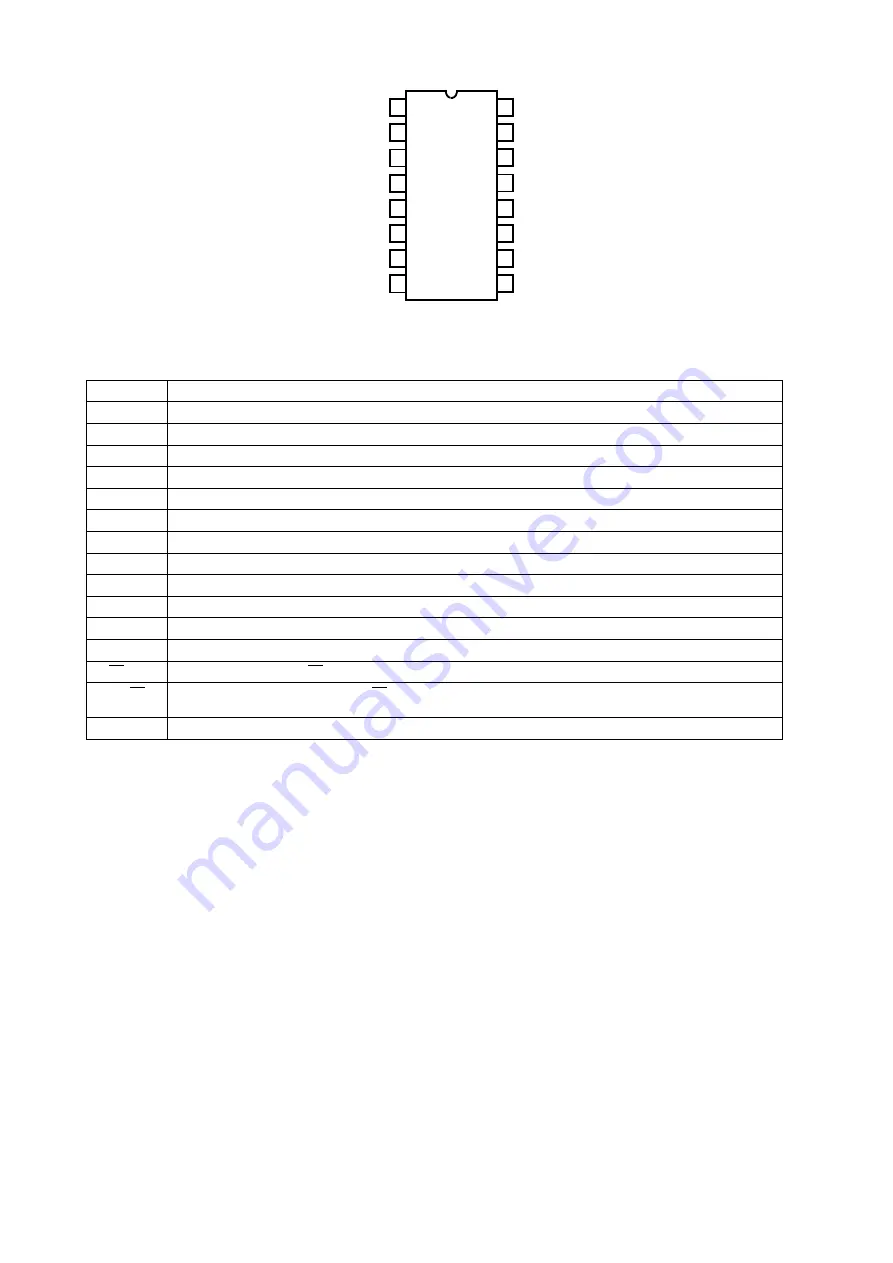
HIN202EIBNZ-T (8U-210094-1 : IC403)
HIN202EIBNZ-T Pin Function
14
15
16
9
13
12
11
10
1
2
3
4
5
7
6
8
C1+
V+
C1-
C2+
C2-
R2
IN
T2
OUT
V
CC
T1
OUT
R1
IN
R1
OUT
T1
IN
T2
IN
R2
OUT
GND
V-
PIN
FUNCTION
V
CC
Power Supply Input 5V 10%, (5V 5% HIN207E).
V+
Internally generated positive supply (+10V nominal).
V-
Internally generated negative supply (-10V nominal).
GND
Ground Lead. Connect to 0V.
C1+
External capacitor (+ terminal) is connected to this lead.
C1-
External capacitor (- terminal) is connected to this lead.
C2+
External capacitor (+ terminal) is connected to this lead.
C2-
External capacitor (- terminal) is connected to this lead.
T
IN
Transmitter Inputs. These leads accept TTL/CMOS levels. An internal 400k
pull-up resistor to V
CC
is connected to each lead.
T
OUT
Transmitter Outputs. These are RS-232 levels (nominally 10V).
R
IN
Receiver Inputs. These inputs accept RS-232 input levels. An internal 5k
pull-down resistor to GND is connected to each input.
R
OUT
Receiver Outputs. These are TTL/CMOS levels.
EN, EN
Receiver Enable Input. With EN = 5V (HIN213E EN=0V), the receiver outputs are placed in a high impedance state.
SD, SD
Shutdown Input. With SD = 5V (HIN213E SD = 0V), the charge pump is disabled, the receiver outputs are in a high impedance
state (except R4 and R5 of HIN213E) and the transmitters are shut off.
NC
No Connect. No connections are made to these leads.
Summary of Contents for UD8004
Page 30: ...26 TROUBLE SHOOTING 1 8U 210095 7 AUDIO UNIT 8U 210094 2 AUDIO2 UNIT 8U 210094 3 AUDIO3 UNIT...
Page 31: ...27...
Page 32: ...28 2 8U 210094 1 POWER UNIT 2 1 The power cannot be turned on...
Page 33: ...29...
Page 34: ...30 3 8U 210095 4 FRONT UNIT 3 1 FL TUBE dosen t light...
Page 35: ...31 4 8U 310041 MAIN UNIT 4 1 No System Power up or Loading No Video or Audio Output...
Page 36: ...32 4 2 No Ether net Operation 4 3 No SD Card Operation...
Page 37: ...33 5 8U 210095 1 ANALOG VIDEO UNIT 5 1 Video S Video Out does not be outputted...
Page 38: ...34 5 2 Component Out does not be outputted...
Page 39: ...35 6 8U 310037 FE SACD UNIT 6 1 BD or DVD or CD or SACD check...
Page 42: ...38 R5F364VDNFB 8U 310041 IC853 R5F364VDNFB Block Diagram...
Page 43: ...39 R5F364VDNFB Pin Function...
Page 44: ...40...
Page 53: ...49 2 FL DISPLAY FL TUBE 15 BT 114GNK 8U 210095 4 FL101...
Page 54: ...50 MEMO...
Page 56: ...54 PRINTED WIRING BOARDS 8U 210094 AUDIO POWER P W B UNIT 1 2 COMPONENT SIDE...
Page 57: ...55 8U 210086 AUDIO POWER P W B UNIT 2 2 FOIL SIDE...
Page 58: ...56 8U 210095 AUDIO POWER VIDEO FRONT P W B UNIT 1 2 COMPONENT SIDE...
Page 59: ...57 8U 210095 AUDIO POWER VIDEO FRONT P W B UNIT 2 2 FOIL SIDE...
Page 60: ...58 8U 310041 MAIN P W B UNIT 1 2 COMPONENT SIDE...
Page 61: ...59 8U 310041 MAIN P W B UNIT 2 2 FOIL SIDE...
Page 62: ...60 8U 310037 FE SACD P W B UNIT FOIL SIDE COMPONENT SIDE...
Page 100: ...96 MEMO...
Page 101: ...97 WIRING DIAGRAM...
Page 105: ...101 PACKING VIEW 201 204 205 207 212 209 208 210 211 z...
Page 146: ...UD8004 8 7 6 5 4 3 2 1 A B C D E F SCHEMATIC DIAGRAMS 34 36 8U 210095 3 SD UNIT...


