Copyright © 2009 Marvell
Doc. No. MV-S105540-00, Rev. --
March 4, 2009, Advance
Document Classification: Proprietary Information
Page 13
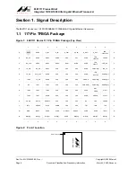
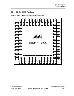
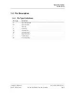
Signal Description
Pin Description
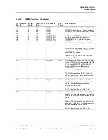
J2
J1
H3
H1
H2
G3
G2
F1
20
19
18
17
16
14
12
11
29
28
26
25
24
20
19
18
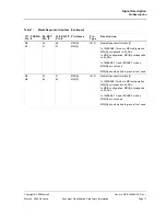
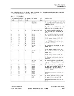
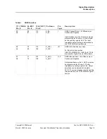
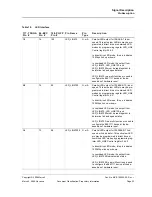
TXD[7]
TXD[6]
TXD[5]
TXD[4]
TXD[3]/TXD[3]
TXD[2]/TXD[2]
TXD[1]/TXD[1]
TXD[0]/TXD[0]
I
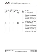
GMII and MII Transmit Data. In GMII mode,
TXD[7:0] present the data byte to be trans-
mitted onto the cable in 1000BASE-T mode.
In MII mode, TXD[3:0] present the data nib-
ble to be transmitted onto the cable in
100BASE-TX and 10BASE-T modes.
TXD[7:4] are ignored in these modes, but
should be driven either high or low. These
pins must not float.
TXD[7:0] are synchronous to GTX_CLK, and
synchronous to TX_CLK in 100BASE-TX
and 10BASE-T modes.
Inputs TXD[7:4] should be tied low if not
used (e.g., RGMII mode).
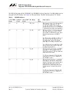
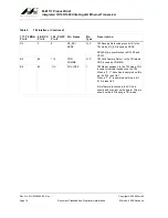
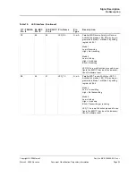
C1
2
7
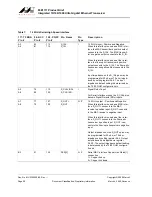
RX_CLK
O, Z
GMII and MII Receive Clock. RX_CLK pro-
vides a 125 MHz clock reference for RX_DV,
RX_ER, and RXD[7:0] in 1000BASE-T
mode, a 25 MHz clock reference in
100BASE-TX mode, and a 2.5 MHz clock
reference in 10BASE-T mode.
TX_TCLK comes from the RX_CLK pins
used in jitter testing. Refer to Register 9 for
jitter test modes.
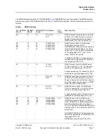
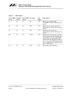
B1
94
4
RX_DV
O, Z
GMII and MII Receive Data Valid. When
RX_DV is asserted, data received on the
cable is decoded and presented on
RXD[7:0] and RX_ER.
RX_DV is synchronous to RX_CLK.
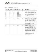
D2
3
8
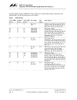
RX_ER
O, Z
GMII and MII Receive Error. When RX_ER
and RX_DV are both asserted, the signals
indicate an error symbol is detected on the
cable.
When RX_ER is asserted with RX_DV de-
asserted, a false carrier or carrier extension
symbol is detected on the cable.
RX_ER is synchronous to RX_CLK.
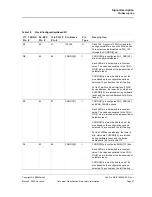
Table 2:
GMII/MII Interfaces (Continued)
117-TFBGA
Pin #
96-BCC
Pin #
128-PQFP
Pin #
Pin Name
Pin
Type
Description


