DS508UM1
43
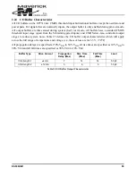
2.15.1.3
DAI Signals
MCLK
oversampled clock. Used as an input to the EP7312 for generating the DAI timing. This sig-
nal is also usually used as an input to a DAC/ADC as an oversampled clock. This signal is
fixed at 256 times the audio sample frequency.
SCLK
bit clock. Used as the bit clock input into the DAC/ADC. This signal is fixed at 128 or
64 times the audio sample frequency.
LRCK
Frame sync. Used as a frame synchronization input to the DAC/ADC. This signal is fixed
at the audio sample frequency. This signal is clocked out on the negative going edge of
SCLK.
SDOUT
Digital audio data out. Used for sending playback data to a DAC. This signal is clocked out
on the negative going edge of the SCLK output.
SDIN
Digital audio input. Used for receiving record data from an ADC. This signal is latched by
the EP7312 on the positive going edge of SCLK.
2.15.2
ADC Interface — Master Mode Only SSI1 (Synchronous Serial Interface)
The first synchronous serial interface allows interfacing to the following peripheral devices:
•
In the default mode, the device is compatible with the MAXIM MAX148/9 in external clock mode.
Similar SPI- or Microwire-compatible devices can be connected directly to the EP7312.
•
In the extended mode and with negative-edge triggering selected (the ADCCON and ADCCKNSEN
bits are set, respectively, in the SYSCON3 register), this device can be interfaced to Analog Devices’
AD7811/12 chip using nADCCS as a common RFS/TFS line.
•
Other features of the devices, including power management, can be utilized by software and the use of
the GPIO pins.
MSB
LRCK
SCLK
Left Channel
Right Channel
SDATA
+3 +2 +1
+5 +4
-1 -2 -3 -4 -5
+3 +2 +1
+5 +4
-1 -2 -3 -4
SDATA
+3 +2 +1
+5 +4
-1 -2 -3 -4 -5
+3 +2 +1
+5 +4
-1 -2 -3 -4
SDATAI
+3 +2 +1
+5 +4
-1 -2 -3 -4 -5
+3 +2 +1
+5 +4
-1 -2 -3 -4
O
128 SCLKs
MSB
MSB
MSB
LSB
LSB
LSB
LSB
Figure 8. EP7312 Rev B- Digital Audio Interface Timing – MSB / Left Justified format
Summary of Contents for EP7312
Page 8: ...DS508UM1 9 Part I EP7312 User s Manual...
Page 58: ...DS508UM1 59 Part II Pin and Register Reference...
Page 122: ......


