60
DS508UM1
4. PIN DESCRIPTIONS
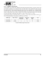
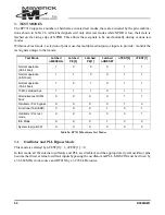
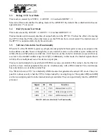
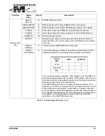
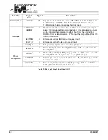
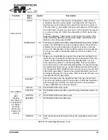
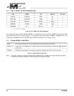
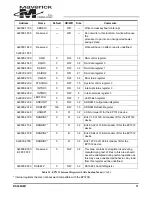
Table 29 describes the function of all external signals to the EP7312. Note that all output signals and all
I/O pins (when acting as outputs) are three stateable. This is to enable the Hi-Z test modes to be supported.
4.1
External Signal Functions
Function
Signal
Name
Signal
Description
Data bus
D[0-31]
I/O
32-bit system data bus for memory, SDRAM, and I/O interface
Address bus
A[0-14]
I/O
15 bits of system byte address during memory and expansion cycles
A[13-27] /
DRA[0-14]
I/O
DRA[0-14] are multiplexed with A[13-27], offering additional power
savings since the lightest loading is expected on the high order ROM
address lines.
Whenever the EP7312 is in the Standby State, the external address
and data buses are driven low. The RUN signal is used internally to
force these buses to be driven low. This is done to prevent peripherals
that are powered-down from draining current. Also, the internal periph-
eral’s signals get set to their Reset State
.
Table 29. External Signal Functions
Summary of Contents for EP7312
Page 8: ...DS508UM1 9 Part I EP7312 User s Manual...
Page 58: ...DS508UM1 59 Part II Pin and Register Reference...
Page 122: ......


