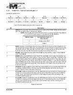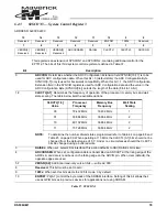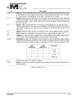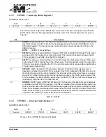
90
DS508UM1
See the “AC Electrical Specification
”
section in the
EP7312 Data Sheet
for more details on bus timing.
The memory area decoded by CS[6] is reserved for the on-chip SRAM, hence this does not require
a configuration field in MEMCFG2. It is automatically set up for 32-bit-wide, no-wait-state accesses.
For the Boot ROM, it is automatically set up for 8-bit, no wait state accesses.
Chip selects nCS[4] and nCS[5] are used to select two CL-PS6700 PC CARD controller devices.
These have a multiplexed 16-bit wide address / data interface, and the configuration bytes in the
MEMCFG2 register have no meaning when these interfaces are enabled.
6.5
Timer / Counter Registers
6.5.1
TC1D — Timer Counter 1 Data Register
ADDRESS: 0x8000.0300
The timer counter 1 data register is a 16-bit read / write register which sets and reads data to TC1.
Any value written will be decremented on the next rising edge of the clock.
6.5.2
TC2D — Timer Counter 2 Data Register
ADDRESS: 0x8000.0340
The timer counter 2 data register is a 16-bit read / write register which sets and reads data to TC2.
Any value written will be decremented on the next rising edge of the clock.
6.5.3
RTCDR — Real Time Clock Data Register
ADDRESS: 0x8000.0380
The Real Time Clock data register is a 32-bit read / write register, which sets and reads the binary
time in the RTC. Any value written will be incremented on the next rising edge of the 1 Hz clock. This
register is reset only by nPOR.
6.5.4
RTCMR — Real Time Clock Match Register
ADDRESS: 0x8000.03C0
The Real Time Clock match register is a 32-bit read / write register, which sets and reads the binary
match time to RTC. Any value written will be compared to the current binary time in the RTC, if they
match it will assert the RTCMI interrupt source. This register is reset only by nPOR.
6.6
LEDFLSH Register
ADDRESS: 0x8000.22C0
The output is enabled whenever LEDFLSH[6] = 1. When enabled, PDDDR[0] needs to be configured
as an output pin and the bit cleared to ‘0’ (See
“PDDDR — Port D Data Direction Register”
.) When
the LED Flasher is disabled, the pin defaults to being used as Port D bit 0. Thus, this will ensure that
the LED will be off when disabled.
6
5-2
1-0
Enable
Duty ratio
Flash rate
Summary of Contents for EP7312
Page 8: ...DS508UM1 9 Part I EP7312 User s Manual...
Page 58: ...DS508UM1 59 Part II Pin and Register Reference...
Page 122: ......


