92
DS508UM1
6.8
SDRFPR — SDRAM Refresh Period Register
ADDRESS: 0x8000.2340
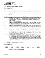
This 16-bit R/W register sets the interval between SDRAM refresh commands. The value pro-
grammed is the interval in BLCK cycles e.g. for a 16
µ
s refresh period with a BCLK of 36MHz, the
following value should be programmed:
16x10
-6
* 36x10
6
= 576
The refresh timer is set to 256 by nPOR to ensure a refresh time of better than 16
µ
s even at 13 MHz.
This register should not be programmed to a value below 2 otherwise the internal bus may become
locked.
This register replaces DPFPR, which is no longer active. Writes to this register are ignored. Reads
from this register will produce unpredictable results.
6.9
UNIQID Register
0x8000.2440
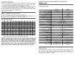
This 32-bit register is set at the factory and is used to implement the MaverickKey™ functionality and
to create
32-bit unique SDMI-assigned IDs. The unique number is read-only and cannot be modified by software.
6.10
RANDID0 Register
8000.2700
This 32-bit register is set at the factory and is used to implement the MaverickKey™ functionality and
to create
128-bit unique random IDs. The unique number is read-only and cannot be modified by software.
9
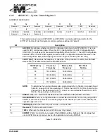
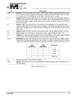
Control over the SDRAM clock. ‘0’=> SDRAM clock is permanently enabled except when in
standby mode. ‘1’=>SDRAM clock stops when the EP7312 is put into inactive mode i.e., SDAC-
TIVE = ‘0’, or when EP7312 is in standby mode.
10
Enables the SDRAM controller: ‘0’ disables, ‘1’ enables. The SDRAM controller will only initialize
if SDACTIVE is set to 1. After initialization, resetting this parameter will cause the SDRAM con-
troller to enter an inactive state. It will remain in this state until SDACTIVE is set to 1.
11-31
Reserved
31-16
15-0
Reserved
REFRATE
31-0
31-0
Bit
Description
Summary of Contents for EP7312
Page 8: ...DS508UM1 9 Part I EP7312 User s Manual...
Page 58: ...DS508UM1 59 Part II Pin and Register Reference...
Page 122: ......


