


DS3234
Extremely Accurate SPI Bus RTC
with Integrated Crystal and SRAM
Maxim Integrated | 10
www.maximintegrated.com
date, month, and year information. The date at the end
of the month is automatically adjusted for months with
fewer than 31 days, including corrections for leap year.
The clock operates in either the 24-hour or 12-hour for-
mat with
AM
/PM indicator. Access to the internal regis-
ters is possible through an SPI bus interface.
A temperature-compensated voltage reference and
comparator circuit monitors the level of V
CC
to detect
power failures and to automatically switch to the backup
supply when necessary. When operating from the back-
up supply, access is inhibited to minimize supply cur-
rent. Oscillator, time and date, and TCXO operations can
continue while the backup supply powers the device.
The
RST
pin provides an external pushbutton function
and acts as an indicator of a power-fail event.
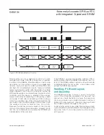
Operation
The block diagram shows the main elements of the
DS3234. The eight blocks can be grouped into four
functional groups: TCXO, power control, pushbutton
function, and RTC. Their operations are described sep-
arately in the following sections.
32kHz TCXO
The temperature sensor, oscillator, and control logic
form the TCXO. The controller reads the output of the
on-chip temperature sensor and uses a lookup table to
determine the capacitance required, adds the aging
correction in the AGE register, and then sets the
capacitance selection registers. New values, including
changes to the AGE register, are loaded only when a
change in the temperature value occurs. The tempera-
ture is read on initial application of V
CC
and once every
64 seconds (default, see the description for CRATE1
and CRATE0 in the
Control/Status Register section)
afterwards.
Power Control
The power control function is provided by a tempera-
ture-compensated voltage reference and a comparator
circuit that monitors the V
CC
level. The device is fully
accessible and data can be written and read when V
CC
is greater than V
PF
. However, when V
CC
falls below
both V
PF
and V
BAT
, the internal clock registers are
blocked from any access. If V
PF
is less than V
BAT
, the
device power is switched from V
CC
to V
BAT
when V
CC
drops below V
PF
. If V
PF
is greater than V
BAT
, the
device power is switched from V
CC
to V
BAT
when V
CC
drops below V
BAT
. After V
CC
returns above both V
PF
and V
BAT
, read and write access is allowed after
RST
goes high (Table 1).
To preserve the battery, the first time V
BAT
is applied to
the device, the oscillator does not start up until V
CC
crosses V
PF
. After the first time V
CC
is ramped up, the
oscillator starts up and the V
BAT
source powers the
oscillator during power-down and keeps the oscillator
running. When the DS3234 switches to V
BAT
, the oscil-
lator may be disabled by setting the
EOSC
bit.
V
BAT
Operation
There are several modes of operation that affect the
amount of V
BAT
current that is drawn. When the part is
powered by V
BAT
, timekeeping current (I
BATT
), which
includes the averaged temperature conversion current,
I
BATTC
, is drawn (refer to Application Note 3644:
Power
Considerations for Accurate Real-Time Clocks for
details). Temperature conversion current, I
BATTC
, is
specified since the system must be able to support the
periodic higher current pulse and still maintain a valid
voltage level. Data retention current, I
BATTDR
, is the
current drawn by the part when the oscillator is
stopped (
EOSC
= 1). This mode can be used to mini-
mize battery requirements for times when maintaining
time and date information is not necessary, e.g., while
the end system is waiting to be shipped to a customer.
Pushbutton Reset Function
The DS3234 provides for a pushbutton switch to be
connected to the
RST
output pin. When the DS3234 is
not in a reset cycle, it continuously monitors the
RST
signal for a low going edge. If an edge transition is
detected, the DS3234 debounces the switch by pulling
the
RST
low. After the internal timer has expired
(PB
DB
), the DS3234 continues to monitor the
RST
line.
If the line is still low, the DS3234 continuously monitors
the line looking for a rising edge. Upon detecting
release, the DS3234 forces the
RST
pin low and holds it
low for t
RST
.
The same pin,
RST
, is used to indicate a power-fail
condition. When V
CC
is lower than V
PF
, an internal
power-fail signal is generated, which forces the
RST
pin
low. When V
CC
returns to a level above V
PF
, the
RST
pin is held low for t
REC
to allow the power supply to sta-
bilize. If the
EOSC
bit is set to logic 1 (to disable the
oscillator in battery-backup mode), tREC is bypassed
and
RST
immediately goes high.
S
UPPLY CONDITION
READ/WRITE
ACCE
SS
ACTIVE
S
UPPLY
RST
V
CC
< V
PF
, V
CC
< V
BAT
No
V
BAT
Active
V
CC
< V
PF
, V
CC
> V
BAT
Yes
V
CC
Active
V
CC
> V
PF
, V
CC
< V
BAT
Yes
V
CC
Inactive
V
CC
> V
PF
, V
CC
> V
BAT
Yes
V
CC
Inactive
Table 1. Power Control