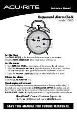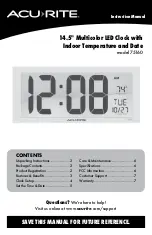


DS3234
Extremely Accurate SPI Bus RTC
with Integrated Crystal and SRAM
Maxim Integrated | 8
www.maximintegrated.com
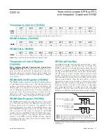
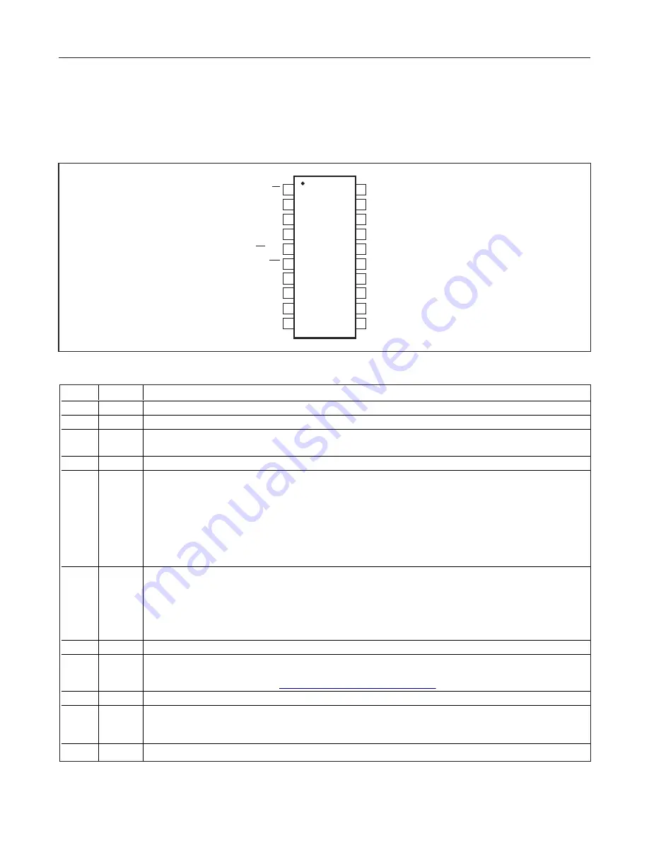
Pin Description
PIN
NAME
FUNCTION
1
CS
Active-Low Chip Select Input. Used to select or deselect the device.
2, 7–14
N.C.
No Connection. Not connected internally. Must be connected to ground.
3
32kHz
32kHz Push-Pull Output. If disabled with either EN32kHz = 0 or BB32kHz = 0, the state of the 32kHz pin will be
low.
4
V
CC
DC Power Pin for Primary Power Supply. This pin should be decoupled using a 0.1µF to 1.0µF capacitor.
5
INT
/SQW
Active-Low Interrupt or Square-Wave Output. This open-drain pin requires an external pullup resistor. It can be
left open if not used. This multifunction pin is determined by the state of the INTCN bit in the Control Register
(0Eh). When INTCN is set to logic 0, this pin outputs a square wave and its frequency is determined by RS2
and RS1 bits. When INTCN is set to logic 1, then a match between the timekeeping registers and either of the
alarm registers activates the
INT
/SQW pin (if the alarm is enabled). Because the INTCN bit is set to logic 1
when power is first applied, the pin defaults to an interrupt output with alarms disabled. The pullup voltage can
be up to 5.5V, regardless of the voltage on V
CC
. If not used, this pin can be left unconnected.
6
RST
Active-Low Reset. This pin is an open-drain input/output. It indicates the status of V
CC
relative to the
V
PF
specification. As V
CC
falls below V
PF
, the
RST
pin is driven low. When V
CC
exceeds V
PF
, for t
RST
, the
RST
pin is driven high impedance. The active-low, open-drain output is combined with a debounced pushbutton
input function. This pin can be activated by a pushbutton reset request. It has an internal 50k
_
nominal value
pullup resistor to V
CC
. No external pullup resistors should be connected. On first power-up, or if the crystal
oscillator is disabled, t
RST
is bypassed and
RST
immediately goes high.
15
GND
Ground
16
V
BAT
Backup Power-Supply Input. If V
BAT
is not used, connect to ground. Diodes placed in series between the V
BAT
pin and the battery can cause improper operation. UL recognized to ensure against reverse charging when
used with a lithium battery. Go to
www.maximintegrated.com/qa/info/ul
.
17
DIN
SPI Data Input. Used to shift address and data into the device.
18, 20
SCLK
SPI Clock Input. Used to control timing of data into and out of the device. Either clock polarity can be used. The
clock polarity is determined by the device based on the state of SCLK when
CS
goes low. Pins 18 and 20 are
electrically connected together internally.
19
DOUT
SPI Data Output. Data is output on this pin when the device is in read mode; CMOS push-pull driver.
TOP VIEW
20
19
18
17
16
15
14
13
1
2
3
4
5
6
7
8
SCLK
DOUT
SCLK
DIN
V
CC
32kHz
N.C.
CS
V
BAT
GND
N.C.
N.C.
N.C.
N.C.
RST
INT/SQW
12
11
9
10
N.C.
N.C.
N.C.
N.C.
SO
DS3234
Pin Configuration