7
◎
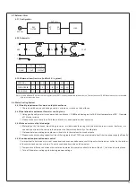
DA, DB and –V(signal) are connected mutually in parallel.
If the lines of CN55 are too long, they should be twisted in pairs to avoid noise.
1 2 3
ON
OFF
Module
No.
Module
No.
1
1
A0
A0
0
1
2
3
4
5
6
7
2
2
A1
A1
3
3
A2
A2
ON
ON
ON
ON
OFF
OFF
OFF
OFF
ON
ON
ON
ON
OFF
OFF
OFF
OFF
ON
ON
ON
ON
OFF
OFF
OFF
OFF
Device address
Device address
DIP switch position
DIP switch position
Table 3-1
3.13 1
.
PMBus Addressing
◎
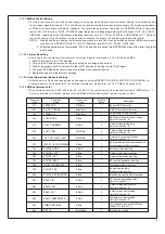
Each PHP-3500 unit should have their unique and own device address to communicate over the PMbus. 7-bit address
setting pins are used to assign a device address for a PHP-3500 unit, as shown in the description below.
A0- A2 allow users to designate an address for PHP-3500 units; these three bits are defined through a 3-pole DIP switch
on the terminal end of
the unit. There are up to 8 different addresses are available to be assigned. When DIP switch in the
"ON" position means logic "0"; when it is in the "OFF" position, meaning logic "1", for example, position 3 in "OFF", the
corresponding bit, A2, is set to logic "1". Please refer to Table 3-1 for the detailed setup advice.
3.12
Auxiliary Output
3.13
PMBus Communication Interface
◎
Built-in 12V/0.5A auxiliary output.
◎
PHP-3500 is compliant with PMBus Rev.1.1, the maximum communication speed is 100KHz and it has the capability of
identifying up to 8 addressed units
.
◎
PMBus communication interface is able to provide the current operating status and information as followings:
1.
.
Output voltage, current and internal temperature
2.
Alarm and status.
3.
Manufacture and model data.
1
MSB
0
0
0
A2
A1
A0
LSB
DA
DA
DA
DA
DB
DB
DB
DB
PHP-3500
PHP-3500
PHP-3500
PHP-3500
+V
-V
LOAD
PSU2 CN55
PSU3 CN55
PSU4 CN55
PSU1 CN55
Fig 6.1
2
2
2
2
14
14
14
14
16
16
16
16
TB1
TB1
TB1
TB1
-V
-V
-V
-V
+V
+V
+V
+V
DA
DA
DA
DA
DB
DB
DB
DB
-V(signal)
-V(signal)
-V(signal)
-V(signal)
+V(signal)
+V(signal)
+V(signal)
+V(signal)
PSU1
PSU2
PSU3
PSU4
13
13
13
13
1
1
1
1
15
15
15
15


