background image

PCI-2515 User's Guide 

Functional Details 

23  

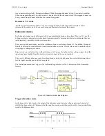
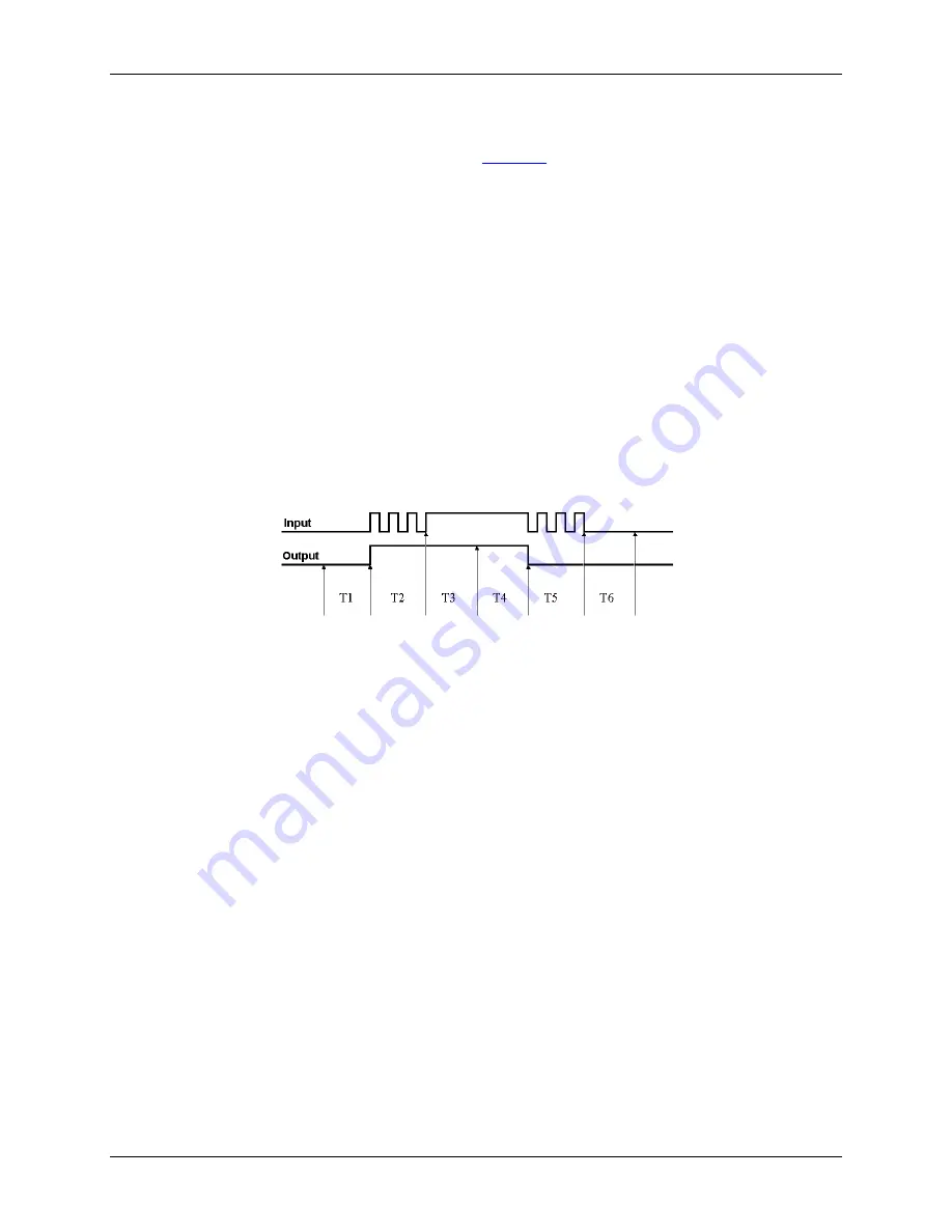
Figure 4-6. Debounce module – trigger after stable mode 

The following time periods (T1 through T5) pertain to 

Figure 4-6

. In 

trigger after stable

 mode, the input signal 

to the debounce module is required to have a period of stability after an incoming edge, in order for that edge to 
be accepted (passed through to the counter module.) The debounce time for this example is equal to T2 and T5. 

ƒ


T1 – In the example above, the input signal goes high at the beginning of time period T1, but never stays 
high for a period of time equal to the debounce time setting (equal to T2 for this example.) 

ƒ


T2 – At the end of time period T2, the input signal has transitioned high and stayed there for the required 
amount of time—therefore the output transitions high. If the input signal does not stabilize in the high state 
long enough, no transition would have appeared on the output and the entire disturbance on the input would 
have been rejected. 

ƒ


T3 – During time period T3, the input signal remained steady. No change in output is seen. 

ƒ


T4 – During time period T4, the input signal has more disturbances and does not stabilize in any state long 
enough. No change in the output is seen. 

ƒ


T5 – At the end of time period T5, the input signal has transitioned low and stayed there for the required 
amount of time—therefore the output goes low. 

Trigger before stable mode 

In the 

trigger before stable

 mode, the output of the debounce module immediately changes state, but will not 

change state again until a period of stability has passed. For this reason the mode can be used to detect glitches. 


Figure 4-7. Debounce module – Trigger before stable mode 

The following time periods (T1 through T6) pertain to the above drawing. 

ƒ


T1 – In the illustrated example, the input signal is low for the debounce time (equal to T1); therefore when 
the input edge arrives at the end of time period T1, it is accepted and the output (of the debounce module) 
goes high. Note that a period of stability must precede the edge in order for the edge to be accepted. 

ƒ


T2 – During time period T2, the input signal is not stable for a length of time equal to T1 (the debounce 
time setting for this example.) Therefore, the output stays "high" and does not change state during time 
period T2. 

ƒ


T3 – During time period T3, the input signal is stable for a time period equal to T1, meeting the debounce 
requirement. The output is held at the high state. This is the same state as the input. 

ƒ


T4 – At anytime during time period T4, the input can change state. When this happens, the output will also 
change state. At the end of time period T4, the input changes state, going low, and the output follows this 
action [by going low]. 

ƒ


T5 – During time period T5, the input signal again has disturbances that cause the input to not meet the 
debounce time requirement. The output does not change state. 

ƒ


T6 – After time period T6, the input signal has been stable for the debounce time and therefore any edge on 
the input after time period T6 is immediately reflected in the output of the debounce module. 

Debounce mode comparisons 

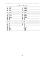
Figure 4-8 shows how the two modes interpret the same input signal, which exhibits glitches. Notice that the 

trigger before stable

 mode recognizes more glitches than the 

trigger after stable 

mode. Use the 

bypass

 option to 

achieve maximum glitch recognition. 

Summary of Contents for PCI-2515

Page 1: ......

Page 2: ...PCI 2515 User s Guide Document Revision 1 September 2006 Copyright 2006 Measurement Computing Corporation ...

Page 3: ... Computing Corporation that is damaged even due to misuse for only 50 of the current list price I O boards face some tough operating conditions some more severe than the boards are designed to withstand When a board becomes damaged just return the unit with an order for its replacement at only 50 of the current list price We don t need to profit from your misfortune By the way we honor this warran...

Page 4: ...is granted by implication or otherwise under any patent or copyrights of Measurement Computing Corporation All rights reserved No part of this publication may be reproduced stored in a retrieval system or transmitted in any form by any means electronic mechanical by photocopying recording or otherwise without the prior written permission of Measurement Computing Corporation Notice Measurement Comp...

Page 5: ... O operations 11 Connectors cables main I O connector 11 Pin out main I O connector 12 Cabling 12 Field wiring and signal termination 13 Chapter 3 Programming and Developing Applications 14 Programming languages 14 Packaged applications programs 14 Chapter 4 Functional Details 15 PCI 2515 block diagram 15 Synchronous I O mixing analog digital and counter scanning 15 Bus mastering DMA 16 Analog inp...

Page 6: ... per PC 25 Chapter 5 Calibrating the PCI 2515 26 Chapter 6 Specifications 27 Analog input 27 Accuracy 27 Analog outputs 28 Digital input output 28 Counters 29 Input sequencer 29 Trigger sources and modes 30 Frequency pulse generators 30 Power consumption 30 PCI compatibility 30 Environmental 31 Mechanical 31 Main connector and pin out 31 ...

Page 7: ...ton italic text Italic text is used for the names of manuals and help topic titles and to emphasize a word or phrase For example The InstaCal installation procedure is explained in the Quick Start Guide Never touch the exposed pins or circuit connections on the board Where to find more information The following electronic documents provide information that can help you get the most out of your PCI...

Page 8: ... output range of 10V to 10V The board has 24 high speed lines of digital I O two timer outputs and four 32 bit counters It provides up to 12 MHz scanning on all digital input lines You can operate all analog I O digital I O and counter timer I O synchronously and simultaneously Software features For information on the features of InstaCal and the other software included with your PCI 2515 refer to...

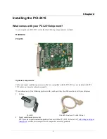
Page 9: ...e with the PCI 2515 are not included with PCI 2515 orders and must be ordered separately If you ordered any of the following products with your board they should be included with your shipment Cables CA 68 3R CA 68 3S 3 feet and CA 68 6S 6 feet Signal conditioning accessories MCC provides signal termination products for use with the PCI 2515 Refer to the Field wiring and signal termination section...

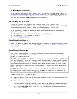
Page 10: ...are The PCI 2515 board is completely plug and play There are no switches or jumpers to set on the board Configuration is controlled by your system s BIOS Before you install the PCI 2515 Enable Bus Mastering DMA For a PCI 2515 to operate properly you must enable Bus Mastering DMA on the PCI slot where you will install the board Make sure that your computer can perform Bus Mastering DMA for the appl...

Page 11: ...e analog input configuration 16 single ended or eight differential channels and the edge used for pacing when using an external clock Once selected any program that uses the Universal Library initializes the hardware according to these selections Information on signal connections General information regarding signal connection and configuration is available in the Guide to Signal Connections This ...

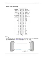
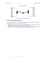
Page 12: ...6 ACH6 HI ACH14 ACH6 LO 58 24 AGND ACH7 57 23 ACH15 NC 56 22 XDAC0 NC 55 21 XDAC1 NEGREF 54 20 POSREF GND 53 19 5V A1 52 18 A0 A3 51 17 A2 A5 50 16 A4 A7 49 15 A6 B1 48 14 B0 B3 47 13 B2 B5 46 12 B4 B7 45 11 B6 C1 44 10 C0 C3 43 9 C2 C5 42 8 C4 C7 41 7 C6 GND 40 6 TTL TRG CNT1 39 5 CNT0 CNT3 38 4 CNT2 TMR1 37 3 TMR0 GND 36 2 XAPCR GND 35 1 XDPCR PCI slot Cabling Use a CA 68 3R 68 pin ribbon expans...

Page 13: ...signals and route them into the PCI 2515 board using the CA 68 3R CA 68 3S or CA 68 6S cable TB 100 Termination board with screw terminals Details on this product are available on our web site at www mccdaq com cbicatalog cbiproduct asp dept_id 98 pf_id 1787 RM TB 100 19 inch rack mount kit for the TB 100 termination board Details on this product are available on our web site at www mccdaq com cbi...

Page 14: ... sm ul user guide pdf Packaged applications programs Many packaged application programs such as SoftWIRE and DASYLab now have drivers for your board If the package you own does not have drivers for the board please fax or e mail the package name and the revision number from the install disks We will research the package for you and advise how to obtain drivers Some application drivers are included...

Page 15: ...l and counter scanning The PCI 2515 can read analog digital and counter inputs while generating up to two analog outputs and digital pattern outputs at the same time Digital and counter inputs do not affect the overall A D rate because these inputs use no time slot in the scanning sequencer For example one analog input channel can be scanned at the full 1 MHz A D rate along with digital and counte...

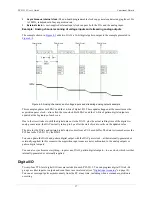
Page 16: ...test mode with a 0 delay between the end of scan and the start of scan a single analog channel can be scanned continuously at 1 MS s two analog channels can be scanned at 500 kS s each 16 analog input channels can be scanned at 62 5 kS s Example Analog channel scanning of voltage inputs Figure 4 2 shows a simple acquisition The scan is programmed pre acquisition and is made up of six analog channe...

Page 17: ...digital data out to the DACs plus the actual settling time of the digital to analog conversion the DACs actually take up to 4 µs after the start of scan to settle on the updated value The data for the DACs and pattern digital output comes from a PC based buffer The data is streamed across the PCI bus to the PCI 2515 by the DMA You can update the DACs and pattern digital output with the DAC pacer c...

Page 18: ...ed in hardware to the analog input level on the selected channel This guarantees an analog trigger latency that is less than 1 µs You can select any analog channel as the trigger channel but the selected channel must be the first channel in the scan You can program the trigger level the rising or falling edge and hysteresis Concerning hardware analog level trigger and comparator change state When ...

Page 19: ...I 2515 avoids this situation by using pre trigger data When software based triggering is used and the PC detects the trigger condition which may be thousands of readings after the actual occurrence of the signal the PCI 2515 driver automatically looks back to the location in memory where the actual trigger causing measurement occurred and presents the acquired data that begins at the point where t...

Page 20: ...into the PCI 2515 Each counter accepts frequency inputs up to 20 MHz The counters can concurrently monitor time periods frequencies pulses and other event driven incremental occurrences directly from pulse generators limit switches proximity switches and magnetic pick ups Counter inputs can be read asynchronously under program control or synchronously as part of an analog or digital scan group Whe...

Page 21: ...nt the upper 16 bits of a 32 bit counter then you can acquire that upper word at the 12 MHz rate The counter counts up and does not clear on every new sample However it does clear at the start of a new scan command The counter rolls over on the 16 bit counter low boundary or on the 32 bit counter high boundary Clear on read mode The counter counts up and is cleared after each read By default the c...

Page 22: ...nce modes as well as a debounce bypass as shown in Figure 4 5 In addition the signal from the buffer can be inverted before it enters the debounce circuitry The inverter is used to make the input rising edge or falling edge sensitive Edge selection is available with or without debounce In this case the debounce time setting is ignored and the input signal goes straight from the inverter or inverte...

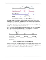
Page 23: ...ason the mode can be used to detect glitches Figure 4 7 Debounce module Trigger before stable mode The following time periods T1 through T6 pertain to the above drawing T1 In the illustrated example the input signal is low for the debounce time equal to T1 therefore when the input edge arrives at the end of time period T1 it is accepted and the output of the debounce module goes high Note that a p...

Page 24: ...groups of glitches and each group is to be counted as one The trigger before stable mode recognizes and counts the first glitch within a group but rejects the subsequent glitches within the group if the debounce time is set accordingly The debounce time should be set to encompass one entire group of glitches as shown in the following diagram Figure 4 9 Optimal debounce time for trigger before stab...

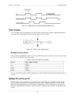
Page 25: ...mples Table 4 3 Timer output frequency examples Divisor Timer output frequency 1 1 MHz 100 10 kHz 1000 1 kHz 10000 100 Hz 65535 15 259 Hz The two timer outputs can generate different square waves The timer outputs can be updated asynchronously at any time Multiple PCI 2515s per PC PCI 2515 features can be replicated up to four times as up to four boards can be installed in a single host PC The ser...

Page 26: ...ion and the other which is available for field calibration You can perform field calibration automatically in seconds with InstaCal and without the use of external hardware or instruments Field calibration derives its traceability through an on board reference which has a stability of 0 005 per year Note that a two year calibration period is recommended for PCI 2515 boards You should calibrate the...

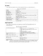
Page 27: ...kHz fundamental Total harmonic distortion 80 dB typical for 10 V range 1 kHz fundamental Calibration Auto calibration calibration factors for each range stored onboard in non volatile RAM CMRR 60 Hz 70 dB typical DC to 1 kHz Bias current 40 pA typical 0 C to 35 C Input impedance 10 MΩ single ended 20 MΩ differential Absolute maximum input voltage 30 V Accuracy Table 2 Analog input accuracy specifi...

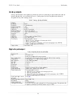
Page 28: ...of input scan Digital input output Table 4 Digital input output specifications Number of I O 24 Ports Three banks of 8 Each port is programmable as input or output Input scanning mode Asynchronous under program control at any time relative to input scanning Configuration 10 kΩ pull up to 5 V 20 pf to analog common Input protection 15 kV ESD clamp diodes Input high 2 0 V to 5 0 V Input low 0 to 0 8...

Page 29: ...unter inputs can be scanned based on either an internal programmable timer or an external clock source Table 6 Input sequencer specifications Scan clock sources two Note 3 Internal Analog channels from 1 µs to 1 sec in 20 83 ns steps Digital channels and counters from 83 33 ns to 1 sec in 20 83 ns steps External TTL level input Analog channels down to 1 µs minimum Digital channels and counters dow...

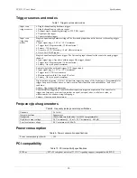
Page 30: ...vel sensitive Minimum pulse width 50 ns high 50 ns low Latency One scan period maximum Digital pattern triggering 8 bit or 16 bit pattern triggering on any of the digital ports Programmable for trigger on equal not equal above or below a value Individual bits can be masked for don t care condition Latency One scan period maximum Input scan triggering modes Counter totalizer triggering Counter tota...

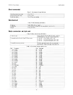
Page 31: ...3R 68 pin ribbon cable 3 feet CA 68 3S 68 pin shielded round cable 3 feet CA 68 6S 68 pin shielded round cable 6 feet TB 100 termination board with screw terminals Compatible accessory products RM TB 100 19 inch rack mount kit for TB 100 Table 14 16 channel single ended pin out Pin Function Pin Function 68 ACH0 34 ACH8 67 AGND 33 ACH1 66 ACH9 32 AGND 65 ACH2 31 ACH10 64 AGND 30 ACH3 63 ACH11 29 AG...

Page 32: ... AGND 62 SGND 28 ACH4 HI 61 ACH4 LO 27 AGND 60 ACH5 HI 26 ACH5 LO 59 AGND 25 ACH6 HI 58 ACH6 LO 24 AGND 57 ACH7 HI 23 ACH7 LO 56 NC 22 XDAC0 55 NC 21 XDAC1 54 NEGREF 20 POSREF 53 GND 19 5V 52 A1 18 A0 51 A3 17 A2 50 A5 16 A4 49 A7 15 A6 48 B1 14 B0 47 B3 13 B2 46 B5 12 B4 45 B7 11 B6 44 C1 10 C0 43 C3 9 C2 42 C5 8 C4 41 C7 7 C6 40 GND 6 TTL TRG 39 CNT1 5 CNT0 38 CNT3 4 CNT2 37 TMR1 3 TMR0 36 GND 2...

Page 33: ...ria A To maintain the safety emission and immunity standards of this declaration the following conditions must be met Part CA 68 3S or CA 68 6S must be properly installed The host computer peripheral equipment power sources and expansion hardware must be CE compliant All I O cables must be shielded with the shields connected to CHASSIS ground stud I O cables must be less than 3 meters 9 75 feet in...

Page 34: ...Measurement Computing Corporation 10 Commerce Way Suite 1008 Norton Massachusetts 02766 508 946 5100 Fax 508 946 9500 E mail info mccdaq com www mccdaq com ...

Reviews: