background image

PCI-DAS1200/JR User's Guide 

Installing the PCI-DAS1200/JR 

14 

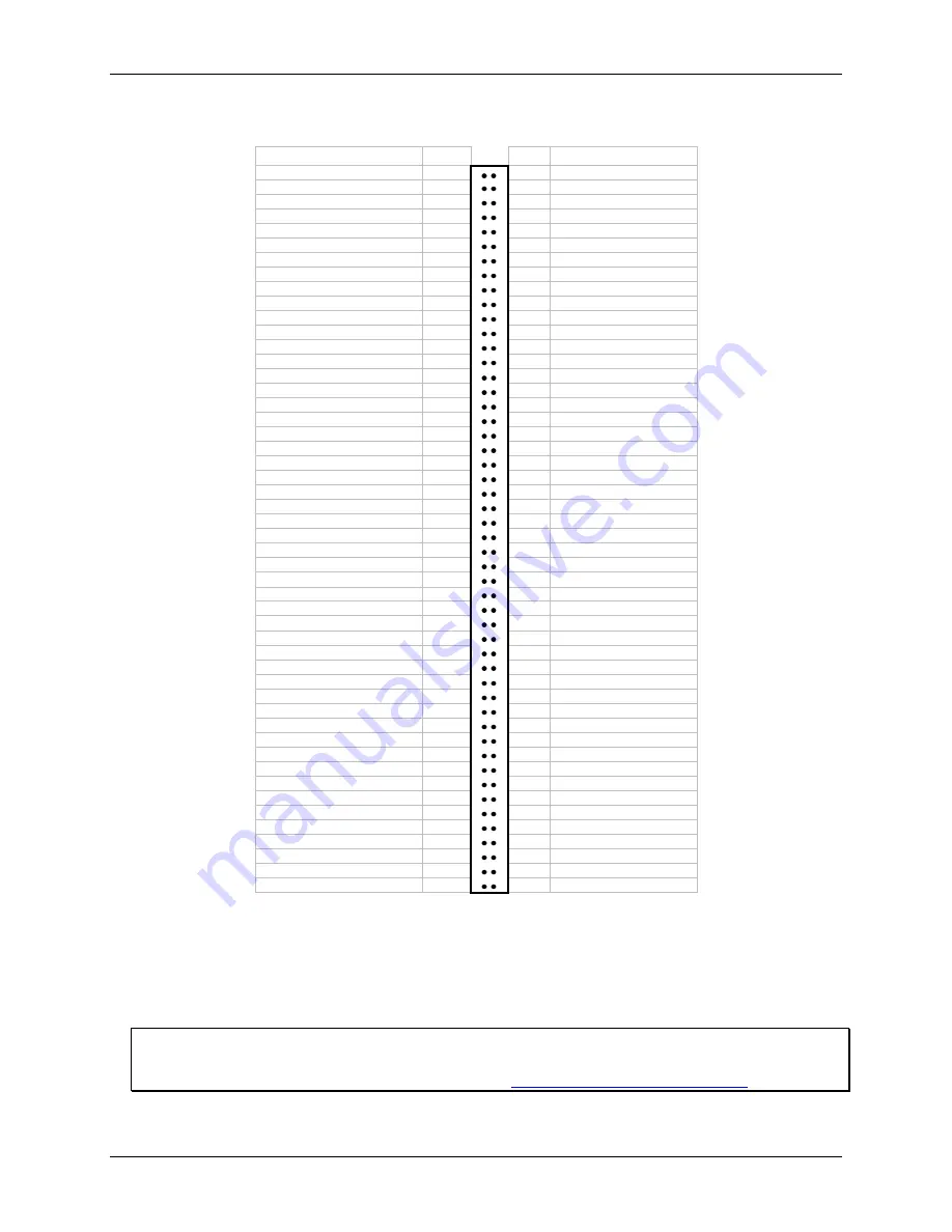
16-channel single-ended mode pin out 

Signal Name 

Pin 


Pin 

Signal Name 

GND 

100 


50 

PC GND 

N/C 

99 


49 

N/C 

N/C 

98 


48 

PC +5V 

N/C 

97 


47 

N/C 

N/C 

96 


46 

N/C 

A/D Internal Pacer Output 

95 


45 

A/D External Trigger 

N/C 

94 


44 

N/C 

N/C 

93 


43 

N/C 

-12V 

92 


42 

A/D External Pacer 

GND 

91 


41 

OUT 4 

+12V 

90 


40 

GATE 4 

GND 

89 


39 

CLK 4 

N/C 

88 


38 

N/C 

CTR5 OUT 

87 


37 

N/C 

CTR5 GATE 

86 


36 

N/C 

CTR5 CLK 

85 


35 

N/C 

N/C 

84 


34 

N/C 

N/C 

83 


33 

N/C 

CTR6 OUT 

82 


32 

N/C 

CTR6 GATE 

81 


31 

N/C 

CTR6 CLK 

80 


30 

N/C 

N/C 

79 


29 

N/C 

N/C 

78 


28 

N/C 

N/C 

77 


27 

N/C 

N/C 

76 


26 

N/C 

N/C 

75 


25 

N/C 

FIRSTPORTC Bit 7 

74 


24 

N/C 

FIRSTPORTC Bit 6 

73 


23 

N/C 

FIRSTPORTC Bit 5 

72 


22 

N/C 

FIRSTPORTC Bit 4 

71 


21 

N/C 

FIRSTPORTC Bit 3 

70 


20 

N/C 

FIRSTPORTC Bit 2 

69 


19 

N/C 

FIRSTPORTC Bit 1 

68 


18 

LLGND 

FIRSTPORTC Bit 0 

67 


17 

CH15 IN 

FIRSTPORTB Bit 7 

66 


16 

CH7 IN 

FIRSTPORTB Bit 6 

65 


15 

CH14 IN 

FIRSTPORTB Bit 5 

64 


14 

CH6 IN 

FIRSTPORTB Bit 4 

63 


13 

CH13 IN 

FIRSTPORTB Bit 3 

62 


12 

CH5 IN 

FIRSTPORTB Bit 2 

61 


11 

CH12 IN 

FIRSTPORTB Bit 1 

60 


10 

CH4 IN 

FIRSTPORTB Bit 0 

59 


CH11 IN 

FIRSTPORTA Bit 7 

58 


CH3 IN 

FIRSTPORTA Bit 6 

57 


CH10 IN 

FIRSTPORTA Bit 5 

56 


CH2 IN 

FIRSTPORTA Bit 4 

55 


CH9 IN 

FIRSTPORTA Bit 3 

54 


CH1 IN 

FIRSTPORTA Bit 2 

53 


CH8 IN 

FIRSTPORTA Bit 1 

52 


CH0 IN 

FIRSTPORTA Bit 0 

51 


LLGND 

PCI slot 


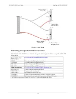
All I/O signals are brought through a 100-pin high-density connector. You can use a C100FF-x to connect field 

signals to the board (Figure 2). This cable has a pair of 50-pin ribbon cables joined at one end to a 100-pin 

connector. The first 50-pin cable (pins 1-50) carries the analog signals. The second 50-pin cable (pins 51-100) 

carries the digital signals. The 100-pin connector mates with the PCI-DAS1200/JR connector. The two 50-pin 

ribbon cables are terminated with standard 50-pin header connectors. 

Information on signal connections 

General information regarding signal connection and configuration is available in the 

Guide to Signal 

Connections

. This document is available on our web site at 

www.mccdaq.com/signals/signals.pdf

). 

Summary of Contents for PCI-DAS1200/JR

Page 1: ......

Page 2: ...PCI DAS1200 JR Multifunction Analog Input and Digital I O User s Guide Document Revision 6 March 2009 Copyright 2009 Measurement Computing Corp ...

Page 3: ...ted in any form by any means electronic mechanical by photocopying recording or otherwise without the prior written permission of Measurement Computing Corporation Notice Measurement Computing Corporation does not authorize any Measurement Computing Corporation product for use in life support systems and or devices without prior written consent from Measurement Computing Corporation Life support d...

Page 4: ...3 ...

Page 5: ... 9 Unpacking the PCI DAS1200 JR 10 Installing the software 10 Installing the hardware 10 Configuring the hardware 11 Differential input mode 11 Single ended input mode 11 Connecting the board for I O operations 11 Connectors cables main I O connector 12 Pin out main I O connector 13 Field wiring and signal termination accessories 15 Chapter 3 Calibrating the board 16 Introduction 16 Calibration th...

Page 6: ...uals and help topic titles and to emphasize a word or phrase For example The InstaCal installation procedure is explained in the Quick Start Guide Never touch the exposed pins or circuit connections on the board Where to find more information The following electronic documents provide helpful information relevant to the operation of the PCI DAS1200 JR board MCC s Specifications PCI DAS1200 JR the ...

Page 7: ...versal Library to control your board Only experienced programmers should try register level programming If you need to program at the register level in your application refer to the Register Map for the PCI DAS1200 Series This document is available at www mccdaq com registermaps RegMapPCI DAS1200 JR pdf ...

Page 8: ...its of parallel digital I O as two 8 bit ports and two 4 bit ports Each port can be configured independently as input or output The PCI DAS1200 JR board contains an 82C54 counter chip which consists of three 16 bit counters Clock gate and output signals from two of the three counters are available on a 100 pin I O connector The third counter is used internally Software features For information on ...

Page 9: ...R FPGA ADC Pacer CTR 2 CTR 1 Sample Counter CTR0 Control Gain and Offset Autocal INT 12 Bit 330KHz Mux Gain Analog In 16 CH S E 8 CH DIFF 1024 x 12 FIFO CTR1 ADC Index Counter User CTR 0 Control Time Base GATE CLK OUT INT XTRIG Start EOC INT 10 MHz PCI Bus 5V 32 bit 33 MHZ Burst Scan Burst Scan EXT PCR 10 MHz CTR2 CLK2 GATE2 OUT2 CLK1 GATE1 OUT1 FIRSTPORTA FIRSTPORTB Control FIRSTPORTCH FIRSTPORTA...

Page 10: ... receive the Quick Start Guide available in PDF at www mccdaq com PDFmanuals DAQ Software Quick Start pdf This booklet supplies a brief description of the software you received with your PCI DAS1200 JR and information regarding installation of that software Please read this booklet completely before installing any software or hardware Optional components If you ordered any of the following product...

Page 11: ...by your system s BIOS To install your board follow the steps below Install the MCC DAQ software before you install your board The driver needed to run your board is installed with the MCC DAQ software Therefore you need to install the MCC DAQ software before you install your board Refer to the Quick Start Guide for instructions on installing the software 1 Turn your computer off open it up and ins...

Page 12: ...nected to LLGND Differential input mode is the preferred configuration for applications in noisy environments or when the signal source is referenced to a potential other than PC ground Single ended input mode When all channels are configured for single ended input mode 16 analog input channels are available In this mode the input signal is referenced to the board s signal ground LLGND The input s...

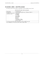
Page 13: ...ype 100 pin high density Compatible cable C100FF x unshielded ribbon cable x length in feet Figure 2 Compatible accessory products with C100FF x cable ISO RACK16 P CIO ERB08 CIO ERB24 CIO SERB24 SSR RACK08 SSR RACK24 BNC 16SE BNC 16DI CIO MINI50 2 required CIO TERM100 1 required SCB 50 1 required These devices require the DADP 5037 PCI DAS to 37 pin SSR and ERB adapter board The CIO ERB08 device a...

Page 14: ... C 77 27 N C N C 76 26 N C N C 75 25 N C FIRSTPORTC Bit 7 74 24 N C FIRSTPORTC Bit 6 73 23 N C FIRSTPORTC Bit 5 72 22 N C FIRSTPORTC Bit 4 71 21 N C FIRSTPORTC Bit 3 70 20 N C FIRSTPORTC Bit 2 69 19 N C FIRSTPORTC Bit 1 68 18 LLGND FIRSTPORTC Bit 0 67 17 CH7 IN LO FIRSTPORTB Bit 7 66 16 CH7 IN HI FIRSTPORTB Bit 6 65 15 CH6 IN LO FIRSTPORTB Bit 5 64 14 CH6 IN HI FIRSTPORTB Bit 4 63 13 CH5 IN LO FIR...

Page 15: ...TPORTB Bit 4 63 13 CH13 IN FIRSTPORTB Bit 3 62 12 CH5 IN FIRSTPORTB Bit 2 61 11 CH12 IN FIRSTPORTB Bit 1 60 10 CH4 IN FIRSTPORTB Bit 0 59 9 CH11 IN FIRSTPORTA Bit 7 58 8 CH3 IN FIRSTPORTA Bit 6 57 7 CH10 IN FIRSTPORTA Bit 5 56 6 CH2 IN FIRSTPORTA Bit 4 55 5 CH9 IN FIRSTPORTA Bit 3 54 4 CH1 IN FIRSTPORTA Bit 2 53 3 CH8 IN FIRSTPORTA Bit 1 52 2 CH0 IN FIRSTPORTA Bit 0 51 1 LLGND PCI slot All I O sig...

Page 16: ...ssories aspx SCB 50 50 conductor shielded signal connection box CIO MINI50 50 pin universal screw terminal accessory BNC 16SE 16 channel single ended BNC connector box BNC 16DI Eight channel differential BNC connector box Signal conditioning http www mccdaq com products signal_conditioning aspx ISO RACK16 P 16 channel isolation module mounting rack SSR RACK24 24 position solid state relay rack SSR...

Page 17: ...the factory Calibration coefficients are stored in nvRAM When using the Universal Library at run time these calibration factors are loaded into system memory and automatically retrieved each time you specify a different DAC ADC range The analog input circuits are calibrated for offset and gain Figure 3 Offset calibration for the analog input is performed directly on the input amplifier PGIA with c...

Page 18: ...l A D External Trigger A D triggering modes External digital Software enabled rising edge hardware trigger Pre trigger Unlimited pre and post trigger samples Total of samples must be 512 Data transfer From 1024 sample FIFO via REPINSW interrupt or software polled A D conversion time 3 µs Throughput 330 kHz min Relative accuracy 1 5 LSB Differential linearity error 0 75 LSB Integral linearity error...

Page 19: ...rupt Counter 1 ADC pacer lower divider Source 10 MHz oscillator Gate tied to counter 2 gate programmable source Output chained to counter 2 clock Counter 2 ADC pacer upper divider Source counter 1 output Gate Tied to counter 1 gate programmable source Output ADC pacer clock if software selected available at user connector 82C54B Counter 0 pretrigger mode Source ADC clock Gate external trigger Outp...

Page 20: ...90 non condensing Main connector and pin out Table 6 I O connector specifications Connector type 100 pin high density Compatible cable C100FF x unshielded ribbon cable x length in feet Compatible accessory products with C100FF x cable ISO RACK16 P CIO ERB08 DADP 5037 adaptor and TN MC78M05CT voltage regulator required CIO ERB24 DADP 5037 adaptor required CIO SERB24 DADP 5037 adaptor required SSR R...

Page 21: ...5 15 CH6 IN LO 65 FIRSTPORTB Bit 6 16 CH7 IN HI 66 FIRSTPORTB Bit 7 17 CH7 IN LO 67 FIRSTPORTC Bit 0 18 LLGND 68 FIRSTPORTC Bit 1 19 N C 69 FIRSTPORTC Bit 2 20 N C 70 FIRSTPORTC Bit 3 21 N C 71 FIRSTPORTC Bit 4 22 N C 72 FIRSTPORTC Bit 5 23 N C 73 FIRSTPORTC Bit 6 24 N C 74 FIRSTPORTC Bit 7 25 N C 75 N C 26 N C 76 N C 27 N C 77 N C 28 N C 78 N C 29 N C 79 N C 30 N C 80 CTR6 CLK 31 N C 81 CTR6 GATE...

Page 22: ...5 FIRSTPORTB Bit 6 16 CH7 IN 66 FIRSTPORTB Bit 7 17 CH15 IN 67 FIRSTPORTC Bit 0 18 LLGND 68 FIRSTPORTC Bit 1 19 N C 69 FIRSTPORTC Bit 2 20 N C 70 FIRSTPORTC Bit 3 21 N C 71 FIRSTPORTC Bit 4 22 N C 72 FIRSTPORTC Bit 5 23 N C 73 FIRSTPORTC Bit 6 24 N C 74 FIRSTPORTC Bit 7 25 N C 75 N C 26 N C 76 N C 27 N C 77 N C 28 N C 78 N C 29 N C 79 N C 30 N C 80 CTR6 CLK 31 N C 81 CTR6 GATE 32 N C 82 CTR6 OUT 3...

Page 23: ...06 IEC 61326 1 2005 EN61000 4 2 2001 Electrostatic Discharge immunity EN61000 4 3 2002 Radiated Electromagnetic Field immunity EN61000 4 4 2004 Electric Fast Transient Burst immunity EN61000 4 5 2001 Surge immunity EN61000 4 6 2003 Radio Frequency Common Mode immunity EN61000 4 11 2004 Voltage Dip and Interrupt immunity Declaration of Conformity based on tests conducted by Chomerics Test Services ...

Page 24: ...Measurement Computing Corporation 10 Commerce Way Suite 1008 Norton Massachusetts 02766 508 946 5100 Fax 508 946 9500 E mail info mccdaq com www mccdaq com ...

Reviews: