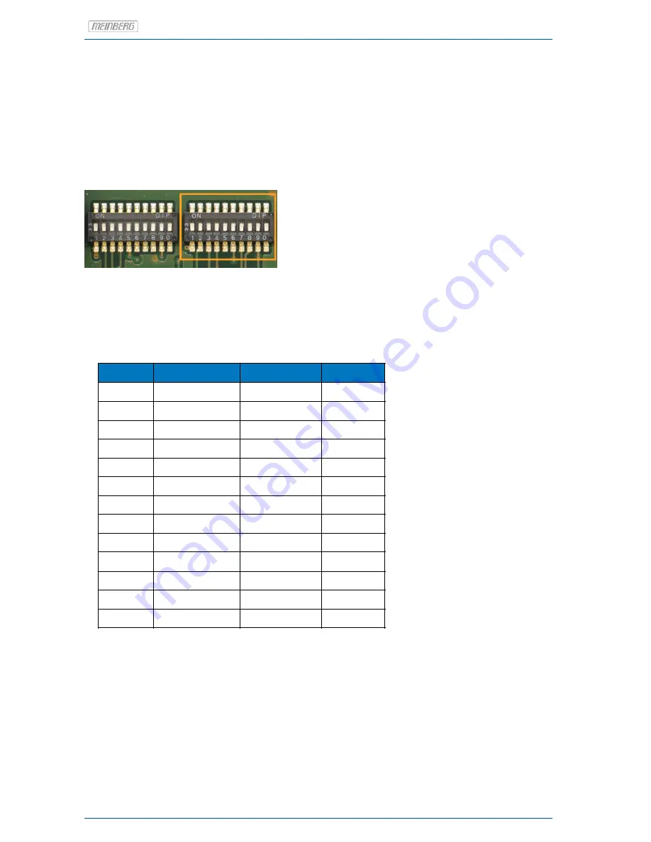
6.1 Configuring the 9 pin connector
By default only the signals needed for the serial port COM0 are mapped to the pins of the connector. Whenever
one of the additional signals shall be used, the signal must be mapped to a pin by putting the appropriate lever
of the DIP switch in the ON position. The table below shows the pin assignments for the connector and the
DIP switch lever assigned to each of the signals. Care must be taken when mapping a signal to Pin 1, Pin 4
or Pin 7 of the connector, because one of two different signals can be mapped to these Pins. Only one switch
may be put in the ON position in this case:
Pin 1:
DIP 1 or DIP 8 ON
Pin 4:
DIP 5 or DIP 10 ON
Pin 7:
DIP 3 or DIP 7 ON
Pin 7:
DIP 6 or DIP 9 ON
———————————————–
The picture on the left shows all DIP switches on po-
sition "OFF". Please use the highlighted block on the
right.
Those signals which do not have a lever of the DIP switch assigned are always available at the connector:
9pin D-SUB
Signal
Signal Level
DIP-Switch
1
VCC out
+5 V
1
1
PPO_0 (PPS) out
RS232
8
2
RxD 0 in
RS232
-
3
TxD 0 out
RS232
-
4
PPO_1 (PPM) out
TTL
5
4
10 MHz out
TTL
10
5
GND
-
-
6
CAP 0 in
TTL
2
7
CAP 1 in
TTL
3
7
IRIG DC out
TTL into 50 ohm
7
8
PPO_0 (PPS) out
TTL
4
9
PPO_2 (DCF) out
TTL
9
9
DCF out
TTL
6
Standard Port
DIP 8 must be OFF
DIP 1 must be OFF
DIP 10 must be OFF
DIP 5 must be OFF
DIP 7 must be OFF
DIP 3 must be OFF
DIP 6 must be OFF
DIP 9 must be OFF
12
Date: 28th March 2018
GPS180PEX


