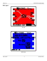
MIC5301/18 Evaluation Board
Single µCap ULDO™
ULDO is a trademark of Micrel, Inc
Micrel Inc. • 2180 Fortune Drive • San Jose, CA 95131 • USA • tel +1 (
408
) 944-0800 • fax + 1 (408) 474-1000 • http://www.micrel.com
March 2007
1
M9999-030707-A
General Description
The demonstration board can be used to evaluate both the
MIC5301 and MIC5318 low dropout linear regulators. The
MIC5301 and MIC5318 are offered in fixed and adjustable
outputs. Fixed output versions add bypass pin function-
ality, allowing reduced output noise. The adjustable
version allows for the use of a resistor divider network to
adjust for the desired output voltage. The evaluation board
accommodates the fixed version.
Requirements
The MIC5301/18 requires a power supply that is able to
deliver 300mA with an input voltage range of 2.3V to 6V.
The output load can be either an active or passive load.
Circuit Description
The MIC5301/18 single Ultra Low Dropout (ULDO™)
linear regulator is easy to use. A minimum output
capacitance of 1µF is required.
An input capacitor is required when the power supply is
more than 4” away from the device. All evaluation boards
include an input capacitor within 1” of the device. This is
the minimum recommended distance from the device that
the capacitor should be placed.
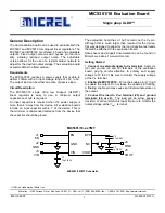
The evaluation board has a 10µF ceramic on the V
IN
pin.
Although this is much larger than required for the device,
this was designed to allow for the long inductive test leads
that will be attached to the evaluation board
Data sheets and support documentation can be found on
Micrel’s web site at: www.micrel.com.
Getting Started
1.
Connect an external supply to V
IN
terminal.
Apply V
IN
(J3) and ground (J2 and J4) terminals of the evaluation
board, paying careful attention to polarity and supply
voltage (2.3V to 6V). Be sure to monitor the supply voltage
at the V
IN
terminal.
2.
Enable the MIC5301/18.
Force the enable pin (J1) high
to enable the output. Do not leave the enable pin floating.
A floating enable pin may cause an indeterminate state on
the output.
3.
Connect the load to V
OUT
terminal (J5) and ground
terminals (J4 or J2).
The load can be either passive
(resistor) or active (electronic load). Be sure to monitor the
output voltage at the V
OUT
terminal.
BYP
EN
GND
J1
EN
MIC5301/18-x.xYMT
VIN
C1
10µF/6.3V
J2
GND
J3
VIN
J4
GND
J5
VOUT
NC
VOUT
C2
0.1µF/25V
C3
1µF/6.3V
MIC5301/18YMT Schematic


