2004 Microchip Technology Inc.
Advance Information
DS70119B-page 131
dsPIC30F6010
20.7
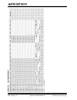
A/D Acquisition Requirements
For the A/D converter to meet its specified accuracy,
the charge holding capacitor (C
HOLD
) must be allowed
to fully charge to the input channel voltage level. The
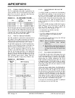
analog input model is shown in Figure 20-2. The
source impedance (R
S
) and the internal sampling
switch (R
SS
) impedance directly affect the time
required to charge the capacitor C
HOLD
. The sampling
switch (R
SS
) impedance varies over the device voltage
(V
DD
), see Figure 20-2. The impedance for analog
sources must be small enough to meet accuracy
requirements at the given speed. After the analog input
channel is selected (changed), this sampling must be
done before the conversion can acquisition sampling
time, Equation 20-2 may be used. This equation
assumes that the input is stepped some multiple (n) of
the LSB step size and the output must be captured to
within 1/2 LSb error (2096 steps for 10-bit A/D).
The C
HOLD
is 4.4 pF for the A/D converter.
EQUATION 20-2: A/D SAMPLING TIME
EQUATIONS
FIGURE 20-2:
ANALOG INPUT MODEL
∆
V
O
=
∆
V
I
• (1 – e (-T
C
/C
HOLD
(R
IC
+R
SS
+R
S
)))
1 – (
∆
V
O
/
∆
V
I
) = e
(-T
C
/C
HOLD
(R
IC
+R
SS
+R
S
))
∆
V
I
= V
IN
– V
REF
-
∆
V
O
= n • LSB – 1/2 LSB
∆
V
O
/
∆
V
I
= (n • LSB – 1/2 LSB) / n • LSB
1 – (
∆
V
O
/
∆
V
I
) = 1 / 2n
1 / 2n
= e (-T
C
/C
HOLD
(R
IC
+R
SS
+R
S
))
T
C
= C
HOLD
• (R
IC
+R
SS
+R
S
) • -In(1/2 • n)
TSMP
= Amplifier Settling Time
+ Holding Capacitor Charging Time (T
C
)
+ Temperature Coefficient †
† The temperature coefficient is only required for
temperatures > 25
°
C.
TSMP
= 0.5
µ
s
+ C
HOLD
• (R
IC
+R
SS
+R
S
) • -In(1/2 • n)
+ [(Temp – 25
°
C)(0.05
µ
s/
°
C)]
C
PIN
VA
Rs
ANx
5 pF
V
T
= 0.6V
V
T
= 0.6V
I leakage
R
IC
≤
250
Ω
Sampling
Switch
SS
R
SS
C
HOLD
= DAC capacitance
V
SS
V
DD
= 4.4 pF
±
500 nA
Legend: C
PIN
V
T
I leakage
R
IC
SS
C
HOLD
= input capacitance
= threshold voltage
= leakage current at the pin due to
= interconnect resistance
= sampling switch
= sample/hold capacitance (from DAC)
various junctions
V
DD
(V)
3.5
2.5
2.0
1.5
1.0
2
3
4
5
(Rss k
Ω
)
Sampling
3.0
0.5
0
6
Switch
Note:
Values shown here are untested typical values, for reference only. Exact electrical specifications are to be determined.
Summary of Contents for dsPIC30F6010
Page 12: ...dsPIC30F6010 DS70119B page 10 Advance Information 2004 Microchip Technology Inc NOTES...
Page 32: ...dsPIC30F6010 DS70119B page 30 Advance Information 2004 Microchip Technology Inc NOTES...
Page 38: ...dsPIC30F6010 DS70119B page 36 Advance Information 2004 Microchip Technology Inc NOTES...
Page 50: ...dsPIC30F6010 DS70119B page 48 Advance Information 2004 Microchip Technology Inc NOTES...
Page 68: ...dsPIC30F6010 DS70119B page 66 Advance Information 2004 Microchip Technology Inc NOTES...
Page 72: ...dsPIC30F6010 DS70119B page 70 Advance Information 2004 Microchip Technology Inc NOTES...
Page 76: ...dsPIC30F6010 DS70119B page 74 Advance Information 2004 Microchip Technology Inc NOTES...
Page 86: ...dsPIC30F6010 DS70119B page 84 Advance Information 2004 Microchip Technology Inc NOTES...
Page 108: ...dsPIC30F6010 DS70119B page 106 Advance Information 2004 Microchip Technology Inc NOTES...
Page 116: ...dsPIC30F6010 DS70119B page 114 Advance Information 2004 Microchip Technology Inc NOTES...
Page 128: ...dsPIC30F6010 DS70119B page 126 Advance Information 2004 Microchip Technology Inc NOTES...
Page 150: ...dsPIC30F6010 DS70119B page 148 Advance Information 2004 Microchip Technology Inc NOTES...
Page 164: ...dsPIC30F6010 DS70119B page 162 Advance Information 2004 Microchip Technology Inc NOTES...
Page 208: ...dsPIC30F6010 DS70119B page 206 Advance Information 2004 Microchip Technology Inc NOTES...
Page 220: ...dsPIC30F6010 DS70119B page 220 Advance Information 2004 Microchip Technology Inc NOTES...
Page 221: ...2004 Microchip Technology Inc Advance Information DS70119B page 221 dsPIC30F6010 NOTES...

