2004 Microchip Technology Inc.
Advance Information
DS70119B-page 163
dsPIC30F6010
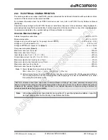
24.0 ELECTRICAL CHARACTERISTICS
This section provides an overview of dsPIC30F electrical characteristics. Additional information will be provided in future
revisions of this document as it becomes available.
For detailed information about the dsPIC30F architecture and core, refer to
dsPIC30F Family Reference Manual
(DS70046).
Absolute maximum ratings for the dsPIC30F family are listed below. Exposure to these maximum rating conditions for
extended periods may affect device reliability. Functional operation of the device at these or any other conditions above
the parameters indicated in the operation listings of this specification is not implied.
Absolute Maximum Ratings
(†)
Ambient temperature under bias............................................................................................................ .-40°C to +125°C
Storage temperature .............................................................................................................................. -65°C to +150°C
Voltage on any pin with respect to V
SS
(except V
DD
and MCLR) ................................................... -0.3V to (V
DD
+ 0.3V)
Voltage on V
DD
with respect to V
SS
......................................................................................................... -0.3V to +5.5V
Voltage on MCLR with respect to V
SS
(Note 1)
......................................................................................... 0V to +13.25V
Total power dissipation
(Note 2)
...............................................................................................................................1.0W
Maximum current out of V
SS
pin ...........................................................................................................................300 mA
Maximum current into V
DD
pin .............................................................................................................................. 250 mA
Input clamp current, I
IK
(V
I
< 0 or V
I
> V
DD
) .......................................................................................................... ±20 mA
Output clamp current, I
OK
(V
O
< 0 or V
O
> V
DD
) ................................................................................................... ±20 mA
Maximum output current sunk by any I/O pin.......................................................................................................... 25 mA
Maximum output current sourced by any I/O pin .................................................................................................... 25 mA
Maximum current sunk by all ports ....................................................................................................................... 200 mA
Maximum current sourced by all ports .................................................................................................................. 200 mA
Note 1:
Power dissipation is calculated as follows:
Pdis = V
DD
x {I
DD
-
∑
I
OH
} +
∑
{(V
DD
- V
OH
) x I
OH
} +
∑
(V
O
l x I
OL
)
2:
Voltage spikes below V
SS
at the MCLR/V
PP
pin, inducing currents greater than 80 mA, may cause latchup.
Thus, a series resistor of 50-100
Ω
should be used when applying a “low” level to the MCLR/V
PP
pin, rather
than pulling this pin directly to V
SS
.
†
NOTICE: Stresses above those listed under “Absolute Maximum Ratings” may cause permanent damage to the
device. This is a stress rating only and functional operation of the device at those or any other conditions above those
indicated in the operation listings of this specification is not implied. Exposure to maximum rating conditions for
extended periods may affect device reliability.
Note:
All peripheral electrical characteristics are specified. For exact peripherals available on specific
devices, please refer the the Family Cross Reference Table.
Summary of Contents for dsPIC30F6010
Page 12: ...dsPIC30F6010 DS70119B page 10 Advance Information 2004 Microchip Technology Inc NOTES...
Page 32: ...dsPIC30F6010 DS70119B page 30 Advance Information 2004 Microchip Technology Inc NOTES...
Page 38: ...dsPIC30F6010 DS70119B page 36 Advance Information 2004 Microchip Technology Inc NOTES...
Page 50: ...dsPIC30F6010 DS70119B page 48 Advance Information 2004 Microchip Technology Inc NOTES...
Page 68: ...dsPIC30F6010 DS70119B page 66 Advance Information 2004 Microchip Technology Inc NOTES...
Page 72: ...dsPIC30F6010 DS70119B page 70 Advance Information 2004 Microchip Technology Inc NOTES...
Page 76: ...dsPIC30F6010 DS70119B page 74 Advance Information 2004 Microchip Technology Inc NOTES...
Page 86: ...dsPIC30F6010 DS70119B page 84 Advance Information 2004 Microchip Technology Inc NOTES...
Page 108: ...dsPIC30F6010 DS70119B page 106 Advance Information 2004 Microchip Technology Inc NOTES...
Page 116: ...dsPIC30F6010 DS70119B page 114 Advance Information 2004 Microchip Technology Inc NOTES...
Page 128: ...dsPIC30F6010 DS70119B page 126 Advance Information 2004 Microchip Technology Inc NOTES...
Page 150: ...dsPIC30F6010 DS70119B page 148 Advance Information 2004 Microchip Technology Inc NOTES...
Page 164: ...dsPIC30F6010 DS70119B page 162 Advance Information 2004 Microchip Technology Inc NOTES...
Page 208: ...dsPIC30F6010 DS70119B page 206 Advance Information 2004 Microchip Technology Inc NOTES...
Page 220: ...dsPIC30F6010 DS70119B page 220 Advance Information 2004 Microchip Technology Inc NOTES...
Page 221: ...2004 Microchip Technology Inc Advance Information DS70119B page 221 dsPIC30F6010 NOTES...

