dsPIC30F6010
DS70119B-page 76
Advance Information
2004 Microchip Technology Inc.
13.1
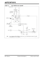
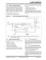
Timer2 and Timer3 Selection Mode
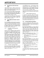
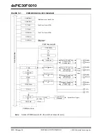
Each output compare channel can select between one
of two 16-bit timers; Timer2 or Timer3.
The selection of the timers is controlled by the OCTSEL
bit (OCxCON<3>). Timer2 is the default timer resource
for the Output Compare module.
13.2
Simple Output Compare Match
Mode
When control bits OCM<2:0> (OCxCON<2:0>) =
001
,
010
or
011
, the selected output compare channel is
configured for one of three simple Output Compare
Match modes:
• Compare forces I/O pin low
• Compare forces I/O pin high
• Compare toggles I/O pin
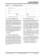
The OCxR register is used in these modes. The OCxR
register is loaded with a value and is compared to the
selected incrementing timer count. When a compare
occurs, one of these Compare Match modes occurs. If
the counter resets to zero before reaching the value in
OCxR, the state of the OCx pin remains unchanged.
13.3
Dual Output Compare Match Mode
When control bits OCM<2:0> (OCxCON<2:0>) =
100
or
101
, the selected output compare channel is config-
ured for one of two Dual Output Compare modes,
which are:
• Single Output Pulse mode
• Continuous Output Pulse mode
13.3.1
SINGLE PULSE MODE
For the user to configure the module for the generation
of a single output pulse, the following steps are
required (assuming timer is off):
• Determine instruction cycle time T
CY
.
• Calculate desired pulse width value based on T
CY
.
• Calculate time to start pulse from timer start value
of 0x0000.
• Write pulse width start and stop times into OCxR
and OCxRS compare registers (x denotes
channel 1, 2, ...,N).
• Set timer period register to value equal to, or
greater than, value in OCxRS compare register.
• Set OCM<2:0> =
100
.
• Enable timer, TON (TxCON<15>) =
1
.
To initiate another single pulse, issue another write to
set OCM<2:0> =
100
.
13.3.2
CONTINUOUS PULSE MODE
For the user to configure the module for the generation
of a continuous stream of output pulses, the following
steps are required:
• Determine instruction cycle time T
CY
.
• Calculate desired pulse value based on T
CY
.
• Calculate timer to start pulse width from timer start
value of 0x0000.
• Write pulse width start and stop times into OCxR
and OCxRS (x denotes channel 1, 2, ...,N)
compare registers, respectively.
• Set timer period register to value equal to, or
greater than, value in OCxRS compare register.
• Set OCM<2:0> =
101
.
• Enable timer, TON (TxCON<15>) =
1
.
13.4
Simple PWM Mode
When control bits OCM<2:0> (OCxCON<2:0>) =
110
or
111
, the selected output compare channel is config-
ured for the PWM mode of operation. When configured
for the PWM mode of operation, OCxR is the Main latch
(read only) and OCxRS is the Secondary latch. This
enables glitchless PWM transitions.
The user must perform the following steps in order to
configure the output compare module for PWM
operation:
1.
Set the PWM period by writing to the appropriate
period register.
2.
Set the PWM duty cycle by writing to the OCxRS
register.
3.
Configure the output compare module for PWM
operation.
4.
Set the TMRx prescale value and enable the
Timer, TON (TxCON<15>) =
1
.
13.4.1
INPUT PIN FAULT PROTECTION
FOR PWM
When control bits OCM<2:0> (OCxCON<2:0>) =
111
,
the selected output compare channel is again config-
ured for the PWM mode of operation, with the addi-
tional feature of input fault protection. While in this
mode, if a logic 0 is detected on the OCFA/B pin, the
respective PWM output pin is placed in the high imped-
ance input state. The OCFLT bit (OCxCON<4>) indi-
cates whether a FAULT condition has occurred. This
state will be maintained until both of the following
events have occurred:
• The external FAULT condition has been removed.
• The PWM mode has been re-enabled by writing
to the appropriate control bits.
Summary of Contents for dsPIC30F6010
Page 12: ...dsPIC30F6010 DS70119B page 10 Advance Information 2004 Microchip Technology Inc NOTES...
Page 32: ...dsPIC30F6010 DS70119B page 30 Advance Information 2004 Microchip Technology Inc NOTES...
Page 38: ...dsPIC30F6010 DS70119B page 36 Advance Information 2004 Microchip Technology Inc NOTES...
Page 50: ...dsPIC30F6010 DS70119B page 48 Advance Information 2004 Microchip Technology Inc NOTES...
Page 68: ...dsPIC30F6010 DS70119B page 66 Advance Information 2004 Microchip Technology Inc NOTES...
Page 72: ...dsPIC30F6010 DS70119B page 70 Advance Information 2004 Microchip Technology Inc NOTES...
Page 76: ...dsPIC30F6010 DS70119B page 74 Advance Information 2004 Microchip Technology Inc NOTES...
Page 86: ...dsPIC30F6010 DS70119B page 84 Advance Information 2004 Microchip Technology Inc NOTES...
Page 108: ...dsPIC30F6010 DS70119B page 106 Advance Information 2004 Microchip Technology Inc NOTES...
Page 116: ...dsPIC30F6010 DS70119B page 114 Advance Information 2004 Microchip Technology Inc NOTES...
Page 128: ...dsPIC30F6010 DS70119B page 126 Advance Information 2004 Microchip Technology Inc NOTES...
Page 150: ...dsPIC30F6010 DS70119B page 148 Advance Information 2004 Microchip Technology Inc NOTES...
Page 164: ...dsPIC30F6010 DS70119B page 162 Advance Information 2004 Microchip Technology Inc NOTES...
Page 208: ...dsPIC30F6010 DS70119B page 206 Advance Information 2004 Microchip Technology Inc NOTES...
Page 220: ...dsPIC30F6010 DS70119B page 220 Advance Information 2004 Microchip Technology Inc NOTES...
Page 221: ...2004 Microchip Technology Inc Advance Information DS70119B page 221 dsPIC30F6010 NOTES...

