2004 Microchip Technology Inc.
Advance Information
DS70119B-page 109
dsPIC30F6010
18.2
Enabling and Setting Up UART
18.2.1
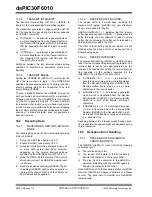
ENABLING THE UART
The UART module is enabled by setting the UARTEN
bit in the UxMODE register (where x = 1 or 2). Once
enabled, the UxTX and UxRX pins are configured as an
output and an input respectively, overriding the TRIS
and LATCH Register bit settings for the corresponding
I/O port pins. The UxTX pin is at logic ‘
1
’ when no
transmission is taking place.
18.2.2
DISABLING THE UART
The UART module is disabled by clearing the
UARTEN bit in the UxMODE register. This is the
default state after any Reset. If the UART is disabled,
all I/O pins operate as port pins under the control of
the latch and TRIS bits of the corresponding port pins.
Disabling the UART module resets the buffers to
empty states. Any data characters in the buffers are
lost, and the baud rate counter is reset.
All error and status flags associated with the UART
module are reset when the module is disabled. The
URXDA, OERR, FERR, PERR, UTXEN, UTXBRK and
UTXBF bits are cleared, whereas RIDLE and TRMT
are set. Other control bits, including ADDEN,
URXISEL<1:0>, UTXISEL, as well as the UxMODE
and UxBRG registers, are not affected.
Clearing the UARTEN bit while the UART is active will
abort all pending transmissions and receptions and
reset the module as defined above. Re-enabling the
UART will restart the UART in the same configuration.
18.2.3
ALTERNATE I/O
The alternate I/O function is enabled by setting the
ALTIO bit (UxMODE<10>). If ALTIO =
1
, the UxATX
and UxARX pins (alternate transmit and alternate
receive pins, respectively) are used by the UART mod-
ule instead of the UxTX and UxRX pins. If ALTIO =
0
,
the UxTX and UxRX pins are used by the UART
module.
18.2.4
SETTING UP DATA, PARITY AND
STOP BIT SELECTIONS
Control bits PDSEL<1:0> in the UxMODE register are
used to select the data length and parity used in the
transmission. The data length may either be 8-bits with
even, odd or no parity, or 9-bits with no parity.
The STSEL bit determines whether one or two stop bits
will be used during data transmission.
The default (Power-on) setting of the UART is 8 bits, no
parity, 1 stop bit (typically represented as 8, N, 1).
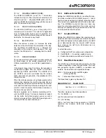
18.3
Transmitting Data
18.3.1
TRANSMITTING IN 8-BIT DATA
MODE
The following steps must be performed in order to
transmit 8-bit data:
1.
Set up the UART:
First, the data length, parity and number of stop
bits must be selected. Then, the Transmit and
Receive Interrupt enable and priority bits are
setup in the UxMODE and UxSTA registers.
Also, the appropriate baud rate value must be
written to the UxBRG register.
2.
Enable the UART by setting the UARTEN bit
(UxMODE<15>).
3.
Set the UTXEN bit (UxSTA<10>), thereby
enabling a transmission.
4.
Write the byte to be transmitted to the lower byte
of UxTXREG. The value will be transferred to the
Transmit Shift register (UxTSR) immediately
and the serial bit stream will start shifting out
during the next rising edge of the baud clock.
Alternatively, the data byte may be written while
UTXEN =
0
, following which, the user may set
UTXEN. This will cause the serial bit stream to
begin immediately because the baud clock will
start from a cleared state.
5.
A Transmit interrupt will be generated depend-
ing on the value of the interrupt control bit
UTXISEL (UxSTA<15>).
18.3.2
TRANSMITTING IN 9-BIT DATA
MODE
The sequence of steps involved in the transmission of
9-bit data is similar to 8-bit transmission, except that a
16-bit data word (of which the upper 7 bits are always
clear) must be written to the UxTXREG register.
18.3.3
TRANSMIT BUFFER (U
X
TXB)
The transmit buffer is 9-bits wide and 4 characters
deep. Including the Transmit Shift Register (UxTSR),
the user effectively has a 5-deep FIFO (First In First
Out) buffer. The UTXBF Status bit (UxSTA<9>)
indicates whether the transmit buffer is full.
If a user attempts to write to a full buffer, the new data
will not be accepted into the FIFO, and no data shift
will occur within the buffer. This enables recovery from
a buffer overrun condition.
The FIFO is reset during any device Reset, but is not
affected when the device enters or wakes up from a
Power Saving mode.
Summary of Contents for dsPIC30F6010
Page 12: ...dsPIC30F6010 DS70119B page 10 Advance Information 2004 Microchip Technology Inc NOTES...
Page 32: ...dsPIC30F6010 DS70119B page 30 Advance Information 2004 Microchip Technology Inc NOTES...
Page 38: ...dsPIC30F6010 DS70119B page 36 Advance Information 2004 Microchip Technology Inc NOTES...
Page 50: ...dsPIC30F6010 DS70119B page 48 Advance Information 2004 Microchip Technology Inc NOTES...
Page 68: ...dsPIC30F6010 DS70119B page 66 Advance Information 2004 Microchip Technology Inc NOTES...
Page 72: ...dsPIC30F6010 DS70119B page 70 Advance Information 2004 Microchip Technology Inc NOTES...
Page 76: ...dsPIC30F6010 DS70119B page 74 Advance Information 2004 Microchip Technology Inc NOTES...
Page 86: ...dsPIC30F6010 DS70119B page 84 Advance Information 2004 Microchip Technology Inc NOTES...
Page 108: ...dsPIC30F6010 DS70119B page 106 Advance Information 2004 Microchip Technology Inc NOTES...
Page 116: ...dsPIC30F6010 DS70119B page 114 Advance Information 2004 Microchip Technology Inc NOTES...
Page 128: ...dsPIC30F6010 DS70119B page 126 Advance Information 2004 Microchip Technology Inc NOTES...
Page 150: ...dsPIC30F6010 DS70119B page 148 Advance Information 2004 Microchip Technology Inc NOTES...
Page 164: ...dsPIC30F6010 DS70119B page 162 Advance Information 2004 Microchip Technology Inc NOTES...
Page 208: ...dsPIC30F6010 DS70119B page 206 Advance Information 2004 Microchip Technology Inc NOTES...
Page 220: ...dsPIC30F6010 DS70119B page 220 Advance Information 2004 Microchip Technology Inc NOTES...
Page 221: ...2004 Microchip Technology Inc Advance Information DS70119B page 221 dsPIC30F6010 NOTES...

