background image

 2015 Microchip Technology Inc.

DS20005459B-page 17

MIC2125/6

4.0

FUNCTIONAL DESCRIPTION

The MIC2125 and MIC2126 are adaptive on-time
synchronous buck controllers built for high input
voltage to low output voltage applications. They are
designed to operate over a wide input voltage range
from 4.5V to 28V and their output is adjustable with an
external resistive divider. An adaptive ON-time control
scheme is employed to obtain a constant switching
frequency and to simplify the control compensation.
Overcurrent protection is implemented when sensing
low-side MOSFET’s R

DS(ON)

. The device features

internal soft-start, enable, UVLO, and thermal
shutdown.

4.1

Theory of Operation

The MIC2125/6 

Functional Block Diagram

 appears on

page two. The output voltage is sensed by the
MIC2125/6 feedback pin (FB), and is compared to a
0.6V reference voltage (V

REF

) at the low gain

transconductance error amplifier (g

m

). 

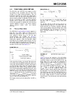
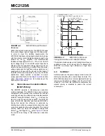
Figure 4-1

shows the MIC2125/6 control loop timing during
steady-state operation. When the feedback voltage
decreases and the amplifier output is below 0.6V, the
comparator triggers and generates an ON-time period.
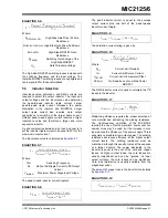
The ON-time period is predetermined by the fixed t

ON

estimator circuitry value from 

Equation 4-1

:

EQUATION 4-1:

At the end of the ON-time, the internal high-side driver
turns off the high-side MOSFET and the low-side driver
turns on the low-side MOSFET. The OFF-time depends
upon the feedback voltage. When the feedback voltage
decreases and the output of the g

m

 amplifier is below

0.6V, the ON-time period is triggered and the OFF-time
period ends. If the OFF-time period determined by the
feedback voltage is less than the minimum OFF-time
t

OFF(min)

, which is about 220 ns, the MIC2125/6 control

logic applies the t

OFF(min)

 instead. t

OFF(min)

 is required

to maintain enough energy in the boost capacitor
(C

BST

) to drive the high-side MOSFET.

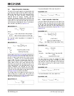
The maximum duty cycle is obtained from the 220 ns
t

OFF(MIN)

:

EQUATION 4-2:

It is not recommended to use MIC2125/6 with an
OFF-time close to t

OFF(MIN)

 during steady-state

operation. 
The adaptive ON-time control scheme results in a
constant switching frequency in the MIC2125/6. The
actual ON-time and resulting switching frequency
varies with the different rising and falling times of the
external MOSFETs. Also, the minimum t

ON

 results in a

lower switching frequency in high V

IN

 to V

OUT

applications. 

FIGURE 4-1:

MIC2125/6 Control Loop 

Timing

Figure 4-2

 shows the operation of the MIC2125/6

during load transient. The output voltage drops due to
a sudden increase in load, which results in the V

FB

falling below V

REF

. This causes the comparator to

trigger an ON-time period. At the end of the ON-time, a
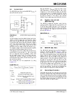
minimum OFF-time t

OFF(min)

 is generated to charge

C

BST

 if the feedback voltage is still below V

REF

. The

next ON-time is triggered immediately after the
t

OFF(min)

 due to the low feedback voltage. This

operation results in higher switching frequency during
load transients. The switching frequency returns to the
nominal set frequency once the output stabilizes at new
load current level. The output recovery time is fast and
the output voltage deviation is small in MIC2125/6
converter due to the varying duty cycle and switching
frequency.

t

ON ESTIMATED

V

OUT

V

IN

f

SW

-----------------------

=

D

MAX

t

S

t

OFF MIN

t

S

-----------------------------------

1

220

ns

t

S

---------------

=

=

Where:

t

S

1/f

SW

Where:

V

OUT

Output Voltage

V

IN

Power Stage Input Voltage

f

SW

Switching Frequency

Summary of Contents for MIC2125

Page 1: ...aptive ON time control architecture The MIC2125 6 operate over an input voltage range from 4 5V to 28V and can be used to supply load current up to 25A The output voltage is adjustable down to 0 6V wi...

Page 2: ...DD AGND EN PG OVP FB FREQ VIN BST DH SW DL PGND ILIM MIC2125 6 4 7 F MIC2125 26 EN VDD EN gm EA COMP CL DETECTION CONTROL LOGIC TIMER SOFT START FIXED TON ESTIMATE UVLO LDO THERMAL SHUTDOWN SOFT START...

Page 3: ...to VIN Notice Stresses above those listed under Absolute Maximum Ratings may cause permanent damage to the device This is a stress rating only and functional operation of the device at those or any o...

Page 4: ...resis 400 mV Load Regulation 0 6 2 3 6 IDD 0 to 40 mA Reference Feedback Reference Voltage 0 597 0 6 0 603 V TJ 25 C 0 5 0 594 0 6 0 606 40 C TJ 125 C 1 FB Bias Current 0 01 0 5 A VFB 0 6V Enable Cont...

Page 5: ...rom low to high PG Hysteresis 6 Sweep VFB from high to low PG Delay Time 80 s Sweep VFB from low to high PG Low Voltage 60 200 mV VFB 90 x VNOM IPG 1 mA Thermal Protection Overtemperature Shutdown 150...

Page 6: ...10s Package Thermal Resistances Thermal Resistance 3 mm x 3 mm QFN 16LD JA 50 8 C W JC 25 3 C W Note 1 The maximum allowable power dissipation is a function of ambient temperature the maximum allowabl...

Page 7: ...vs Input Voltage MIC2125 FIGURE 2 5 Switching Frequency vs Input Voltage FIGURE 2 6 Switching Frequency vs Temperature MIC2126 Note The graphs and tables provided following this note are a statistical...
Page 8: ...DD Voltage vs Input Voltage MIC2125 FIGURE 2 8 Enable Threshold vs Input Voltage MIC2125 FIGURE 2 9 Output Peak Current Limit vs Input Voltage MIC2125 V FIGURE 2 10 VIN Operating Supply Current vs Tem...

Page 9: ...2 13 VIN Shutdown Current vs Temperature MIC2125 FIGURE 2 14 VDD UVLO Threshold vs Temperature MIC2125 FIGURE 2 15 Enable Threshold vs Temperature MIC2125 FIGURE 2 16 EN Bias Current vs Temperature MI...

Page 10: ...PCBn Actual results will depend upon the size of the PCB ambient temperature and proximity to other heat emitting components FIGURE 2 19 Line Regulation vs Temperature MIC2125 FIGURE 2 20 Feedback Vol...

Page 11: ...ctual results will depend upon the size of the PCB ambient temperature and proximity to other heat emitting components FIGURE 2 25 Case Temperature vs Output Current MIC2125 FIGURE 2 26 Efficiency VIN...

Page 12: ...le Turn On Turn Off FIGURE 2 36 Enable Turn On Delay and Rise Time VIN 12V VOUT 1 2V IOUT 20A Time 10ms div IL 20A div VIN 10V div VSW 10V div VOUT 2V div IN VIN 12V VOUT 1 2V IOUT 20A Time 10ms div I...

Page 13: ...into Short Circuit FIGURE 2 42 Output Peak Current Limit Threshold VIN 12V VOUT 1 2V IOUT 20A Time 200 s div IL 20A div VEN 2V div VOUT 1V div VIN 12V VOUT 1 2V IOUT 20A Time 10ms div VEN 1V div VOUT...

Page 14: ...C2125 Switching Waveform IOUT 0 1A VIN 12V VOUT 1 2V IOUT 10A to Short Time 8ms div IL 10A div VOUT 500mV div VIN 12V ILDO 1 2V VIN Short to 10A Time 8ms div IL 10A div VOUT 500mV div p y vin 12V VOUT...

Page 15: ...wer Good at VIN Soft Turn Off VIN 12V VOUT 1 2V IOUT 10A Time 2 s div IL 10A div VSW 5V div VOUT 20mV div AC coupled OUT VIN 12V VOUT 1 2V IOUT 20A Time 2 s div IL 10A div VOUT 20mV div AC Coupled VSW...

Page 16: ...e of the buck converter The SW pin also senses the current by monitoring the voltage across the low side MOSFET during OFF time In order to sense the current accurately connect the low side MOSFET dra...

Page 17: ...OFF time period determined by the feedback voltage is less than the minimum OFF time tOFF min which is about 220 ns the MIC2125 6 control logic applies the tOFF min instead tOFF min is required to ma...

Page 18: ...g comparator ZC detection that monitors the inductor current by sensing the voltage drop across the low side MOSFET during its ON time If the VFB 0 6V and the inductor current goes slightly negative t...

Page 19: ...ng the SW voltage when the low side FET is off If the SW node voltage exceeds 12 mV typical the device turns off the low side FET until the next ON time event is triggered The negative current limit v...

Page 20: ...ETs are essentially equal to the power stage input voltage VIN A safety factor of 30 should be added to the VIN MAX while selecting the voltage rating of the MOSFETs to account for voltage spikes due...

Page 21: ...l and minimizing the winding resistance The high frequency operation of the MIC2125 6 requires the use of ferrite materials Lower cost iron powder cores may be used but the increase in core loss reduc...

Page 22: ...ripple Refer to the Ripple Injection subsection for details The voltage rating of the capacitor should be twice the output voltage for a tantalum and 20 greater for aluminum electrolytic or OS CON Th...

Page 23: ...n the range of 10 k to 49 9 k and calculate R1 using Equation 5 23 EQUATION 5 23 5 8 Ripple Injection The VFB ripple required for proper operation of the MIC2125 6 gm amplifier and comparator is 20 mV...

Page 24: ...SW via a resistor RINJ and a capacitor CINJ as shown in Figure 5 7 FIGURE 5 7 Invisible Ripple at FB The process of sizing the ripple injection resistor and capacitors is as follows Select CINJ as 10...

Page 25: ...o the switch node SW short Do not route any digital lines underneath or close to the inductor Keep the switch node SW away from the feedback FB pin The SW pin should be connected directly to the drain...

Page 26: ...Technology Inc 7 0 PACKAGING INFORMATION 16 Lead QFN 3 mm x 3 mm Package Outline and Recommended Land Pattern Note For the most current package drawings please see the Microchip Packaging Specificatio...

Page 27: ...2015 Microchip Technology Inc DS20005459B page 27 MIC2125 6 Note For the most current package drawings please see the Microchip Packaging Specification located at http www microchip com packaging...

Page 28: ...MIC2125 6 DS20005459B page 28 2015 Microchip Technology Inc...

Page 29: ...9 MIC2125 6 APPENDIX A REVISION HISTORY Revision A November 2015 Original Conversion of this Document Revision B December 2015 Corrected the erroneous listing of the MIC2126 example with a 64LD packag...

Page 30: ...MIC2125 6 DS20005459B page 30 2015 Microchip Technology Inc NOTES...

Page 31: ...ad 40 C to 125 C junction temperature range 16LD QFN b MIC2126YML 28V Synchronous Buck Controller featuring Adap tive On Time Control with Hyper Speed Control 40 C to 125 C junction temperature range...

Page 32: ...MIC2125 6 DS2005459B page 32 2015 Microchip Technology Inc NOTES...

Page 33: ...rademark of Microchip Technology Inc in other countries GestIC is a registered trademark of Microchip Technology Germany II GmbH Co KG a subsidiary of Microchip Technology Inc in other countries All o...

Page 34: ...86 24 2334 2829 Fax 86 24 2334 2393 China Shenzhen Tel 86 755 8864 2200 Fax 86 755 8203 1760 China Wuhan Tel 86 27 5980 5300 Fax 86 27 5980 5118 China Xian Tel 86 29 8833 7252 Fax 86 29 8833 7256 ASI...

Reviews: