Fabric DDR Subsystem
Microsemi ProprietaryUG0446 User Guide Revision 7.0
136
4.4
I/O Utilization
The following table shows the I/O utilization for SmartFusion2 and IGLOO2 devices corresponding to
supported bus widths. The remaining I/Os in bank 0 can be used for general purposes.
Note:
If FDDR is configured for LPDDR, one more IO also available for every 8-bit as the LPDDR doesn't have
DQS_N.
For general purpose use of the unused I/Os in the FDDR bank, select one of the I/O standards with the
same voltage level as the DDR I/Os.
Self refresh must be disabled if the FDDR banks contain a mixed of I/Os used for DDR and for general
purpose fabric I/Os. For more information, see “Self Refresh” in the
"Power Saving Modes" section on
.
4.5
Functional Description
This section provides a detailed description of the FDDR subsystem with the following sub-sections:
•
•
•
•
4.5.1
Architecture Overview
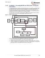
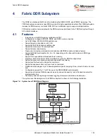
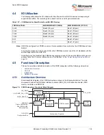
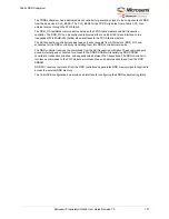
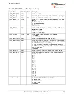
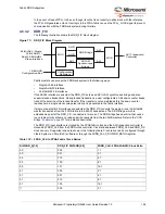
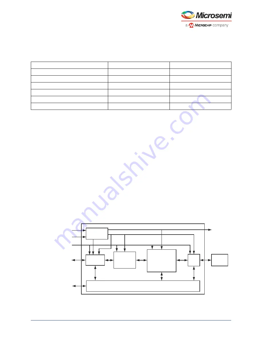
A functional block diagram of the FDDR subsystem is shown in the following illustration. The main
components include the DDR fabric interface controller (DDR_FIC), AXI transaction handler, DDR
memory controller, and DDR PHY.
Figure 75 •
FDDR Subsystem Functional Block Diagram
Table 127 •
I/O Utilization for SmartFusion2 and IGLOO2 Devices
FDDR Bus Width
M2S050/M2GL050 (FG896)
M2S150/M2GL150 (FC1152)
36-bit
Bank5 (85 pins)
Bank1 (85 pins)
32-bit
Bank5 (76 pins)
Bank1 (76 pins)
18-bit
Bank5 (59 pins)
Bank1 (59 pins)
16-bit
Bank5 (53 pins)
Bank1 (53 pins)
9-bit
–
Bank1 (47 pins)
8-bit
–
Bank1 (41 pins)
CLK_BASE
CLK_BASE_PLL_LOCK
CORE_RESET_N
FDDR_CLK
FPLL_LOCK
DDR_FIC
DDR
SDRAM
PHY
Clock
Controller
AXI
Transaction
Controller
DDR Controller
Configuration Registers
64-Bit AXI/
Single 32-Bit AHBL/
Dual 32-Bit AHBL
Slave Interface
16-Bit APB
Configuration Bus
DDR_FIC_CLK


