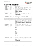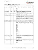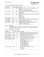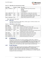
Fabric DDR Subsystem
Microsemi ProprietaryUG0446 User Guide Revision 7.0
150
4.6.3.3.4
Reorder Buffer
The reorder buffer receives data from the DDR controller and orders the data as requested by the AXI
master when a single AXI transaction is split into multiple DDR controller transactions, depending on the
transfer size.
4.6.3.4
DDR Controller
The DDR controller receives requests from the AXI transaction controller, performs the address mapping
from system addresses to DRAM addresses (rank, bank, row, and column) and prioritizes requests to
minimize the latency of reads (especially high priority reads) and maximize page hits. It also ensures that
DRAM is properly initialized, all requests are made to DRAM legally (accounting for associated DRAM
constraints), refreshes are inserted as required, and the DRAM enters and exits various power-saving
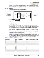
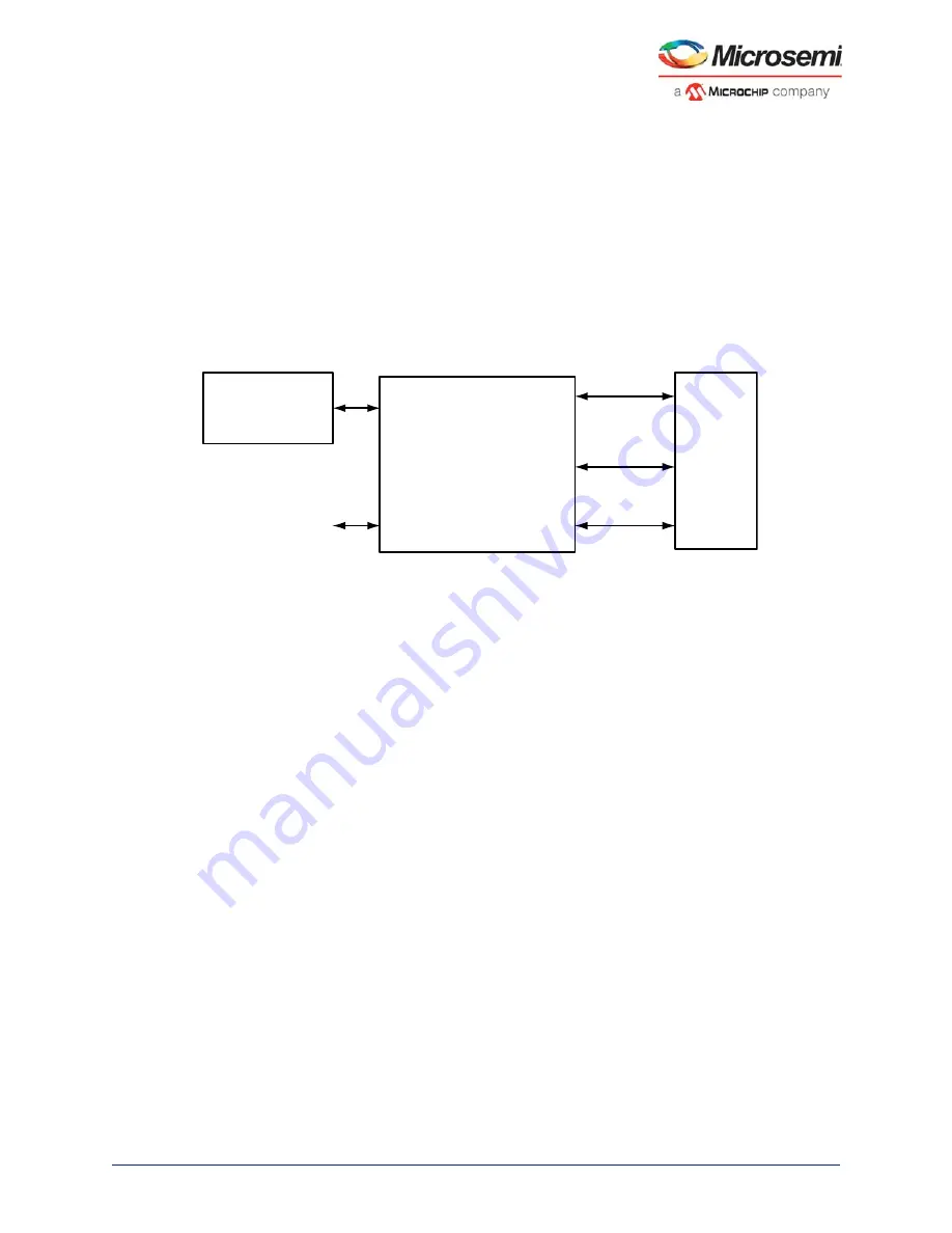
modes appropriately. The following illustration shows the DDR controller connections in the FDDR
subsystem.
Figure 79 •
DDR Controller Block Diagram
The following sections describe key functions of the DDR controller.
4.6.3.4.1
Address Mapping
Read and write requests to the DDR controller requires a system address. The controller is responsible
for mapping this system address with rank, bank, row, and column address to DRAM.
The address mapper maps linear request addresses to DDR memory addresses by selecting the source
bit that maps to each and every applicable DDR memory address bit. The address map interface
registers can be configured to map source address bits to DRAM address (for more information, refer to
page 155 on configuring the FDDR features).
4.6.3.4.2
Transaction Scheduling
The DDR controller schedules the read and write transactions to DDR memory. The DDR controller
classifies the transactions into three types, based on the commands from the AXI transaction controller:
•
Low priority reads (LPR)
•
High priority reads (HPR)
•
Writes (WR)
Each type of transaction has a queue and the queued transactions can be in normal state or in critical
state. The transactions in a queue moves from normal state to critical state when that transaction is not
serviced for a count of MAX_STARVE_X32 clocks. The MAX_STARVE_X32 values for each queue can
be configured using the DDR controller performance registers (refer to the
). The DDR controller completes the critical transactions with high priority.
4.6.3.4.3
Write Combine
The DDR controller combines multiple writes to the same address into a single write to DDR memory.
When a new write collides with the queued write, the DDR controller overwrites the data for the queued
write with that from the new write and only performs one write transaction. The write combine
functionality can be disabled by setting the register bit REG_DDRC_DIS_WC to 1 (
PHY
AXI
Transaction
Controller
16-Bit APB
Register Interface
Control
Interface
Data
Interface
Training
Interface
DDR Controller

