MDDR Subsystem
Microsemi Proprietary UG0446 User Guide Revision 7.0
7
•
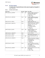
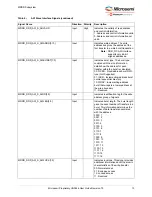
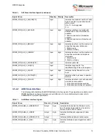
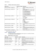
Data line MDDR_DQ_ECC[0] when data width is x8
3.3
Performance
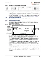
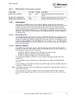
The following table shows the maximum data rates supported by MDDR subsystem for supported
memory types.
For more Information, refer to the "DDR Memory Interface Characteristics" section in
FPGA and SmartFusion2 SoC FPGA Datasheet.
3.4
I/O Utilization
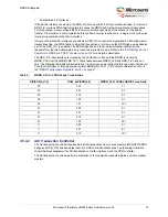
The following table lists the I/O utilization for the SmartFusion2 and IGLOO2 devices corresponding to
supported bus widths. The remaining I/Os in Bank 0 can be used for general purposes.
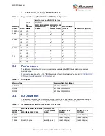
Table 2 •
Supported Memory (DDR2, DDR3 and LPDDR1) Configurations
Memory
Depth
Width
Width
(in
SECDED
Mode)
SmartFusion2 and IGLOO2 Devices
M2S/M2GL
005/010/025/060/090
M2S/M2GL150-
FCV484
M2S/M2GL 050
(FCS325,
VF400, FG484)
M2S/M2GL 050
(FG896)
M2S/M2GL150(FC1152)
128M or
Less
×32
×36
–
–
✔
✔
×16
×18
✔
✔
✔
✔
×8
×9
✔
–
–
✔
256M
×32
×36
–
–
✔
✔
×16
×18
✔
✔
✔
✔
×8
×9
✔
–
–
✔
512M
×32
×36
–
–
✔
✔
×16
×18
✔
✔
✔
✔
×8
×9
✔
–
–
✔
1G
×32
×36
–
–
✔
✔
×16
×18
✔
✔
✔
✔
x8
×9
✔
–
–
✔
Table 3 •
DDR Speeds
Memory Type
Maximum Data Rate (Mbps)
LPDDR1
400 Mbps (200 MHz)
DDR2
667 Mbps (333.33 MHz)
DDR3
667 Mbps (333.33 MHz)
Table 4 •
I/O Utilization for SmartFusion2 and IGLOO2 Devices
MDDR Bus
Width
M2S/M2GL005/010/025/060/0
90
M2S/M2GL150-FCV484
M2S/M2GL 050
(FCS325, VF400,
FG484)
M2S/M2GL 050
(FG896)
M2S/M2GL 150
(FC1152)
36-bit
–
–
Bank0 (85 pins)
Bank2 (85 pins)
32-bit
–
–
Bank0 (76 pins)
Bank2 (76 pins)
18-bit
Bank0 (59 pins)
Bank0 (59 pins)
Bank0 (59 pins)
Bank2 (59 pins)

