Fabric DDR Subsystem
Microsemi ProprietaryUG0446 User Guide Revision 7.0
175
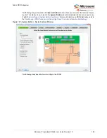
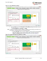
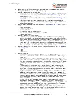
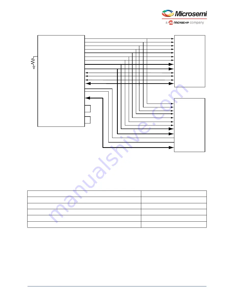
Figure 100 •
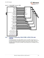
x16 LPDDR1 SDRAM Connection to FDDR
4.9
FDDR Configuration Registers
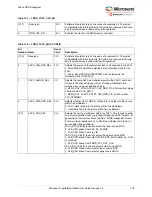
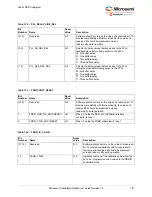
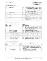
This section provides FDDR subsystem registers along with the address offset, functionality, and bit
definitions. The registers are categorized based on the controller blocks in the FDDR subsystem.
The following table lists the categories of registers and their offset addresses.
Note:
The FDDR SYSREG configuration registers can be locked to prevent them from being overwritten by the
masters that have access to these registers. For information on how to lock/unlock these registers, see
"Appendix B: Register Lock Bits Configuration" on page 204
.
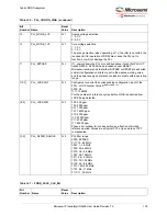
Table 142 •
Address Table for Register Interfaces
Registers
Address Offset Space
DDR Controller Configuration Register,
0x000:0x1FC
PHY Configuration Register Summary,
0x200:0x3FC
DDR_FIC Configuration Register Summary,
0x400:0x4FC
FDDR SYSREG Configuration Register Summary,
0x500:0x5FC
Reserved
0x600:0x7FC
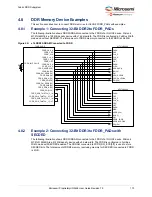
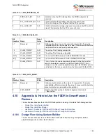
CASN
CKE
CLK_P
CLK_N
CSN
RASN
WEN
ADDR[12:0]
BA[2:0]
MT46H32M16LF
FDDR_CAS_N
FDDR_CKE
FDDR_CLK
FDDR_CLK_N
FDDR_CS_N
FDDR_RAS_N
FDDR_WE_N
FDDR_ADDR[12:0]
FDDR_BA[1:0]
FDDR_DM_RDQS[1:0]
FDDR_DQS[0]
FDDR_DQ[15:0]
DQ[15:0]
UDQS
LDQS
UDM, LDM
CASN
CKE
CLK_P
CLK_N
CSN
RASN
WEN
ADDR[12:0]
BA[2:0]
MT46H32M16LF
DQ[1:0]
LDQS
LDM
FDDR_DM_RDQS_ECC
FDDR_DQS_ECC
FDDR_DQ_ECC[1:0]
FDDR_DQS[1]
FDDR_PADS
FDDR_DQS_TMATCH_0_IN
FDDR_DQS_TMATCH_0_OUT
R
FDDR_IMP_CALIB
FDDR_DQS_TMATCH_ECC_IN
FDDR_DQS_TMATCH_ECC_OUT


