Fabric DDR Subsystem
Microsemi ProprietaryUG0446 User Guide Revision 7.0
178
13
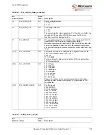
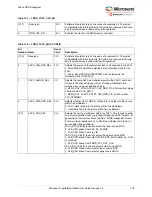
PLL_MODE_3V3
0×1
Analog voltage selection
1: 3.3 V
0: 2.5 V
12
PLL_MODE_1V2
0×1
Core voltage selection
1: 1.2 V
0: 1.0 V
The wrong selection (when operating at 1 V, the jitter is not within the
required limit for operation of DDR) may cause the PLL not to
function, but will not damage the PLL.
11
PLL_BYPASS
0×1
If 1, powers down the PLL core and bypasses it such that PLLOUT
tracks REFCK. BYPASS has precedence over RESET.
Microsemi recommends that either BYPASS or RESET are asserted
until all configuration controls are set in the desired working value,
and the power supply and reference clock are stable within operating
range.
[10:7]
PLL_LOCKCNT
0×F
Configured to control the corresponding configuration input of the
FPLL. LOCK counter Value 2
(binary value + 5)
0000: 32
1111: 1048576
For the number of reference cycles before LOCK is asserted from
LOCK being detected.
[6:4]
PLL_LOCKWIN
0×0
000: 500 ppm
100: 8000 ppm
001: 1000 ppm
101: 16000 ppm
010: 2000 ppm
110: 32000 ppm
011: 4000 ppm
111: 64000 ppm
Phase error window for Lock assertion as a fraction of divided
reference period. Values are at typical PVT only and are not PVT
compensated.
[3:0]
PLL_FILTER_RANGE
0×9
PLL filter range
0000: BYPASS
0111: 18–29 MHz
0001: 1–1.6 MHz
1000: 29–46 MHz
0010: 1.6–2.6 MHz
1001: 46–75 MHz
0011: 2.6–4.2 MHz
1010: 75–120 MHz
0100: 4.2–6.8 MHz
1011: 120–200 MHz
0101: 6.8–11 MHz
0110: 11–18 MHz
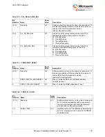
Table 147 •
FDDR_FACC_CLK_EN
Bit
Number
Name
Reset
Value
Description
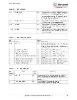
Table 146 •
PLL_CONFIG_HIGH
(continued)
Bit
Number Name
Reset
Value
Description

