MDDR Subsystem
Microsemi Proprietary UG0446 User Guide Revision 7.0
8
Note:
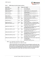
If MDDR is configured for LPDDR, one more IO also available for every 8-bit as the LPDDR does not
have DQS_N.
For general purpose use of the unused I/Os in the MDDR bank, select one of the I/O standards with the
same voltage level as the DDR I/Os.
Self refresh must be disabled if the MDDR banks contain a mixed of I/Os used for DDR and for general
purpose fabric I/Os.For more information, see
"Self Refresh (DDR2, DDR3, LPDDR1)" on page 24
3.5
Functional Description
This section provides the functional description of the MDDR subsystem.
3.5.1
Architecture Overview
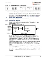
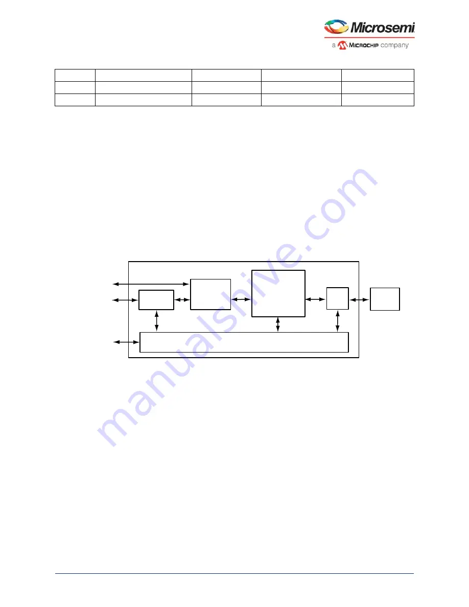
The following illustration shows a functional block diagram of the MDDR subsystem. The main
components include the DDR fabric interface controller (DDR_FIC), AXI transaction handler, DDR
memory controller, and DDR PHY.
Figure 2 •
MDDR Subsystem Functional Block Diagram
The DDR_FIC facilitates communication between the FPGA fabric masters and AXI transaction
controller. The DDR_FIC can be configured to provide either one 64-bit AXI slave interface or two
independent 32-bit AHB-Lite (AHBL) slave interfaces to the FPGA fabric masters.
The AXI transaction controller receives read and write requests from AXI masters (MSS/HPMS DDR
bridge and DDR_FIC) and schedules for the DDR controller by translating them into DDR controller
commands.
The DDR controller receives the commands from the AXI transaction controller. These commands are
queued internally and scheduled for access to the DDR SDRAM while satisfying DDR SDRAM
constraints, transaction priorities, and dependencies between the transactions. The DDR controller in
turn issues commands to the PHY module, which launches and captures data to and from the DDR
SDRAM.
DDR PHY receives commands from the DDR controller and generates DDR memory signals required to
access the external DDR memory.
The 16-bit APB configuration bus provides an interface to configure the MDDR subsystem registers. The
MDDR subsystem operates on MDDR_CLK. MSS/HPMS CCC generates the MDDR_CLK using MPLL.
For more details on MSS/HPMS CCC refer
UG0449: SmartFusion2 and IGLOO2 Clocking Resources
.
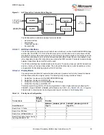
16-bit
Bank0 (53 pins)
Bank0 (53 pins)
Bank0 (53 pins)
Bank2 (53 pins)
9-bit
Bank0 (47 pins)
–
–
Bank2 (47 pins)
8-bit
Bank0 (41 pins)
–
–
Bank2 (41 pins)
Table 4 •
I/O Utilization for SmartFusion2 and IGLOO2 Devices
AXI
Transaction
Controller
DDR Controller
PHY
DDR_FIC
Configuration Registers
16-Bit APB
Configuration Bus
64-Bit AXI /
Single 32-Bit
AHBL / Dual
32-Bit AHBL
Slave Interface
64-Bit AXI
Connected to
MSS/HPMS
DDR Bridge
DDR
SDRAM


