Fabric DDR Subsystem
Microsemi ProprietaryUG0446 User Guide Revision 7.0
188
4.
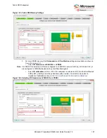
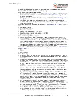
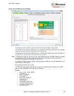
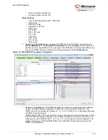
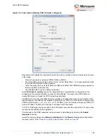
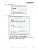
Depending on the application requirement; select the
Memory Initialization
settings under the
Memory Initialization
tab as shown in the following image.
•
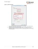
Select the below performance related settings
•
Burst Length can be selected as 4, 8 or 16.
for supported burst lengths.
•
Burst order can be selected as sequential or interleaved. Refer
for
supported burst orders.
•
Timing mode can be selected as 1T or 2T. For more details refer to 1
•
CAS latency is the delay, in clock cycles, between the internal READ command and the
availability of the first bit of output data. Select the CAS latency according to the DDR memory
(Mode register) datasheet.
•
Select the below power saving mode settings. Refer to
"Power Saving Modes" on page 151
details.
•
Self-Refresh Enabled
•
Auto Refresh Burst Count
•
Power down Enabled
•
Stop the clock: supported only for LPDDR
•
Deep Power down Enabled: supported only for LPDDR
•
Power down entry time
•
Select the additional performance settings.
•
Additive CAS Latency is defined by EMR[5:3] register of DDR2 memory and by MR1[4:3]
register of DDR3 memory. It enables the DDR2 or DDR3 SDRAM to allow a READ or WRITE
command from DDR Controller after the ACTIVATE command for the same bank prior to tRCD
(MIN). This configuration is part of DDR2 Extended Mode register and DDR3 Mode register1.
•
CAS Write Latency (CWL) is defined by DDR3 MR2[5:3] and is the delay, in clock cycles, from
the releasing of the internal write to the latching of the first data in. The overall WRITE latency
(WL) is equal to CWL + AL, where CWL is set to 5 clock cycles by default.
•
Select the below ZQ Calibration settings for DDR3 memory. For more details refer
.
•
Zqinit
•
ZQCS
•
ZQCS Interval
•
Select other settings.
•
Local ODT setting is not supported for LPDDR memory. For DDR2/DDR3 memory type, user
can choose any option for “Local ODT”. User can enable or disable “LOCAL ODT” during read
transaction.
•
Drive strength setting is defined by EMR[7:5] register bits of LPDDR memory with drop down
options of `Full', `Half', `Quarter' and `One-eighth' drive strength, it is defined by EMR[1] register
bit of DDR2 memory with drop down options of `Full' and `Weak' drive strength and it is defined
by MR1 register bits M5 and M1 of DDR3 memory with drop down options of `RZQ/6' and
`RZQ/7'.
•
Partial array self-refresh coverage setting is defined by EMR[2:0] register bits of LPDDR
memory with drop down options of `Full', `Quarter', `One-eighth' and `One-sixteenth'. This
feature helps in improving power savings during self-refresh by selecting the amount of memory
to be refreshed during self-refresh.
•
R
TT
(Nominal) setting is defined by EMR[6] and EMR[2] register bits of DDR2 memory which
determines what ODT resistance is enabled with drop down options of `RTT disabled', '50
ohms', '75
Ω
' and `150
Ω
' and it is defined by MR1[9], MR1[6] and MR1[2] register bits of DDR3
memory. In DDR3 memory RTT nominal termination is allowed during standby conditions and
WRITE operations and NOT during READ operations with drop down options of `RZQ/2',
`RZQ/4' and `RZQ/6'.
•
R
TT
_WR (Dynamic ODT) setting is defined by MR2[10:9] register bits of DDR3 memory. This is
applicable only during WRITE operations. If dynamic ODT (Rtt_WR) is enabled, DRAM
switches from normal ODT (R
TT_nom
) to dynamic ODT (Rtt_WR) when beginning WRITE burst
and subsequently switches back to normal ODT at the end of WRITE burst. The drop down
options provided to the user are `off', `RZQ/4' and `RZQ/2'.
•
Auto self-refresh setting is defined by MR2[6] register bit of DDR3 memory with drop down
option of `Manual' and `Auto'.Self-refresh temperature setting is defined by MR2[7] register bit
of DDR2 memory with drop down options of `Normal' and `Extended'.

