MDDR Subsystem
Microsemi Proprietary UG0446 User Guide Revision 7.0
35
•
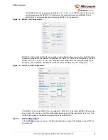
For address mapping, the register settings that perform mapping to system address bits for row,
bank and column combinations are automatically computed by the configurator using the address
mapping option. The following table lists the supported range for row, bank, and column.
For more information refer to the
•
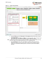
Select the
I/O Drive Strength
as
Half Drive Strength
or
Full Drive Strength,
as shown in
page 36. The following table lists how the DDR I/O standard is configured based on this
setting.
Table 21 •
Supported Address Width Range for Row, Bank and Column Addressing in DDR/LPDDR
Width
DDR2
DDR3
LPDDR
Row Address
12–16
12–16
12–16
Bank Address
2–3
2–3
2–3
Column Address
9–12
9–12
9–12
Table 22 •
DDR I/O Standard is Configured Based on I/O Drive Strength Setting
I/O Drive Strength
Memory Type
DDR2
DDR3
Half Drive Strength
SSTL18I
SSTL15I
Full Drive Strength
SSTL18II
SSTL15II

