MDDR Subsystem
Microsemi Proprietary UG0446 User Guide Revision 7.0
91
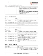
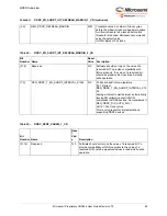
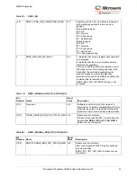
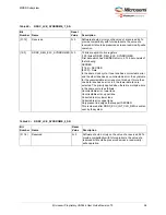
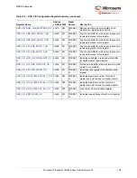
[5:3]
DDRC_CORE_REG_OPERATING_MODE
0×0
Operating mode. This is 3 bits wide in designs
with mobile support and 2-bits in all other
designs.
Non-mobile designs:
000: Init
001: Normal
010: Power-down
011: Self Refresh
Mobile designs:
000: Init
001: Normal
010: Power-down
011: Self refresh
1XX: Deep power-down
0
DDRC_REG_MR_WR_BUSY
0×0
1: Indicates that a mode register write operation
is in progress.
0: Indicates that the core can initiate a mode
register write operation.
Core must initiate an MR write operation only if
this signal is Low. This signal goes High in the
clock after the controller accepts the write
request. It goes Low when the MR write
command is issued to the DRAM. Any MR write
command that is received when
DDRC_REG_MR_WR_BUSY is High, is not
accepted.
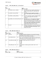
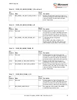
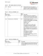
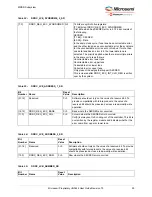
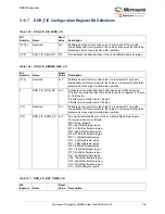
Table 79 •
DDRC_SINGLE_ERR_CNT_STATUS_SR
Bit
Number
Name
Reset
Value
Description
[31:6
Reserved
0×0
Software should not rely on the value of a
reserved bit. To provide compatibility with future
products, the value of a reserved bit should be
preserved across a read-modify-write operation.
[15:0]
DDRC_SINGLE_ERR_CNT_STATUS_REG 0×0
Single error count status.
If the count reaches 0xFFFF, it is held and only
cleared after
DDRC_ECC_INT_CLR_REG
is
written over by the system.
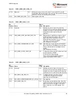
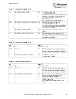
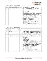
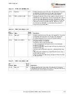
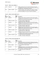
Table 80 •
DDRC_DOUBLE_ERR_CNT_STATUS_SR
Bit
Number Name
Reset
Value
Description
[15:0]
DDRC_DOUBLE_ERR_CNT_STATUS_REG 0×0
Double error count status.
If the count reaches 0xFFFF then it is held and
only cleared after
DDRC_ECC_INT_CLR_REG is written over by
the system.
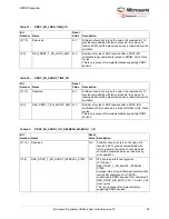
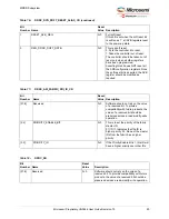
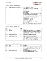
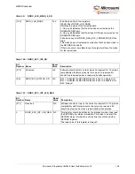
Table 78 •
DDRC_SR


