MDDR Subsystem
Microsemi Proprietary UG0446 User Guide Revision 7.0
95
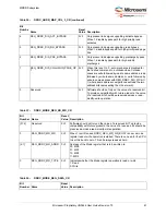
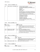
[7:0]
DDRC_REG_ECC_SYNDROMES 0×0
72 bits are split into five registers.
[71:64] bits of DDRC_REG_ECC_SYNDROMES.
First data which has SECDED error in it. 72 bits consists of
the following:
SECDED:
[71:64] – SECDED
[63:00] – Data
In the same clock cycle, if one lane has a correctable error
and the other lane has an uncorrectable error, the
syndrome for the uncorrectable error is sent on this bus. If
more than one data lane has an error in it, the lower data
lane is selected. The priority applied when there are
multiple errors in the same cycle is as follows:
Uncorrectable error, lower lane
Uncorrectable error, upper lane
Correctable error, lower lane
Correctable error, upper lane
Only present in designs that support SECDED.
This is cleared after
DDRC_ECC_INT_CLR_REG is written over by the system.
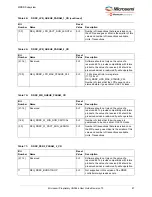
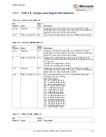
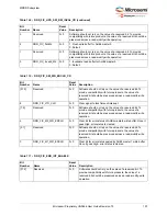
Table 86 •
DDRC_LUE_ADDRESS_1_SR
Bit
Number
Name
Reset
Value
Description
[31:15]
Reserved
0×0
Software should not rely on the value of a reserved bit. To
provide compatibility with future products, the value of a
reserved bit should be preserved across a read-modify-
write operation.
[14:12]
DDRC_REG_ECC_BANK
0×0
Bank where the SECDED error occurred.
Only present in designs that support SECDED.
[11:0]
DDRC_REG_ECC_COL
0×0
Column where the SECDED error occurred.
Col[0] is always set to 0, coming out of the controller. This
bit is overwritten by the register module and indicates
whether the error came from upper or lower lane.
Only present in designs that support SECDED.
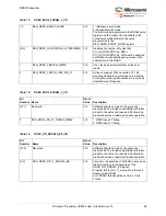
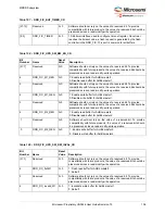
Table 87 •
DDRC_LUE_ADDRESS_2_SR
Bit
Number
Name
Reset
Value
Description
[31:16]
Reserved
0×0
Software should not rely on the value of a reserved bit. To
provide compatibility with future products, the value of a
reserved bit should be preserved across a read-modify-
write operation.
15:0
DDRC_REG_ECC_ROW
0×0
Row where the SECDED error occurred.
Only present in designs that support SECDED.
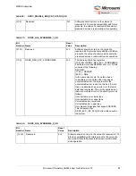
Table 85 •
DDRC_LUE_SYNDROME_5_SR

