MDDR Subsystem
Microsemi Proprietary UG0446 User Guide Revision 7.0
110
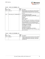
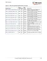
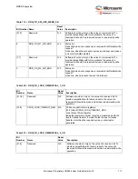
Table 117 •
DDR_FIC_HPD_SW_WRB_EMPTY_SR
Bit
Number
Name
Reset
Value
Description
[31:7]
Reserved
0×0
Software should not rely on the value of a reserved bit. To provide
compatibility with future products, the value of a reserved bit
should be preserved across a read-modify-write operation.
6
DDR_FIC_M1_RBEMPTY
0×0
1: Read buffer of AHBL master1 does not have valid data.
5
Reserved
0×0
Software should not rely on the value of a reserved bit. To provide
compatibility with future products, the value of a reserved bit
should be preserved across a read-modify-write operation.
4
DDR_FIC_M1_WBEMPTY 0×0
1: Write buffer of AHBL master1 does not have valid data.
0: Default
3
Reserved
0×0
Software should not rely on the value of a reserved bit. To provide
compatibility with future products, the value of a reserved bit
should be preserved across a read-modify-write operation.
2
DDR_FIC_M2_RBEMPTY
0×0
1: Read buffer of AHBL master2 does not have valid data.
0: Default.
1
Reserved
0×0
Software should not rely on the value of a reserved bit. To provide
compatibility with future products, the value of a reserved bit
should be preserved across a read-modify-write operation.
0
DDR_FIC_M2_WBEMPTY 0×0
1: Write buffer of AHBL master2 does not have valid data.
0: Default
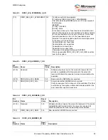
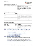
Table 118 •
DDR_FIC_SW_HPB_LOCKOUT_SR
Bit
Number Name
Reset
Value
Description
[31:9]
[7]
[5]
[3]
[1]
Reserved
0×0
Software should not rely on the value of a reserved bit. To provide
compatibility with future products, the value of a reserved bit
should be preserved across a read-modify-write operation.
8
DDR_FIC_LCKTOUT
0×0
Indicates lock counter in arbiter reached its maximum value.
Lock counter (20-bit) starts counting when a locked request gets
access to a bus and will be cleared when the lock signal becomes
logic 0.
6
DDR_FIC_M2_WDSBL_DN
0×0
High indicates AHBL master2 write buffer is disabled.
4
DDR_FIC_M2_RDSBL_DN
0×0
High indicates AHBL master2 read buffer is disabled.
2
DDR_FIC_M1_WDSBL_DN
0×0
High indicates AHBL master1 read buffer is disabled.
0
DDR_FIC_M1_RDSBL_DN
0×0
High indicates AHBL master1 write buffer is disabled.

