Fabric DDR Subsystem
Microsemi ProprietaryUG0446 User Guide Revision 7.0
140
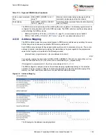
4.5.2.1
AXI Slave Interface
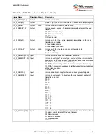
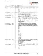
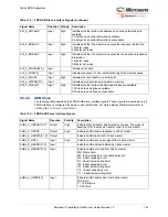
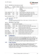
The following table describes the FDDR AXI slave interface signals. These signals are available only if
FDDR interface is configured for AXI mode. For more details of AXI protocol, refer to
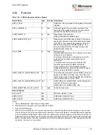
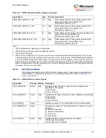
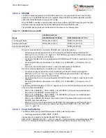
FDDR_DQS_TMATCH_0_OUT
Out
High
DQS enables output for timing match between DQS
and system clock. For simulations, tie to
FDDR_DQS_TMATCH_0_IN.
FDDR_DQS_TMATCH_1_OUT
Out
High
DQS enables output for timing match between DQS
and system clock. For simulations, tie to
FDDR_DQS_TMATCH_1_IN.
FDDR_DQS_TMATCH_ECC_IN
In
High
DQS enables input for timing match between DQS and
system clock. For simulations, tie to
FDDR_DQS_TMATCH_ECC_OUT.
FDDR_DQS_TMATCH_ECC_OUT
Out
High
DQS enables output for timing match between DQS
and system clock. For simulations, tie to
FDDR_DQS_TMATCH_ECC_IN.
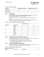
Table 129 •
FDDR AXI Slave Interface Signals
Signal Name
Direction Polarity Description
AXI_S_ARREADY
Output
High
Indicates whether the slave is ready to accept an address and
associated control signals.
1: Slave ready
0: Slave not ready
AXI_S_AWREADY
Output
High
Indicates that the slave is ready to accept an address and associated
control signals.
1: Slave ready
0: Slave not ready
AXI_S_BID[3:0]
Output
Indicates response ID. The identification tag of the write response.
AXI_S_BRESP[1:0]
Output
Indicates write response. This signal indicates the status of the write
transaction.
00: Normal access okay
01: Exclusive access okay
10: Slave error
11: Decode error
AXI_S_BVALID
Output
High
Indicates whether a valid write response is available.
1: Write response available
0: Write response not available.
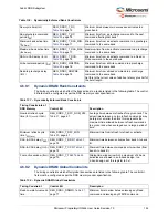
Table 128 •
FDDR Subsystem Interface Signals
(continued)
Signal Name
Type
Polarity Description
Notes:
1. *AXI or AHB interface, depending on configuration.
2. FDDR_DQS_N[3:0] signals are not available for LPDDR.
3. Only in IGLOO2 Devices.
4. TMATCH_IN and TMATCH_OUT pins are required to be connected together outside the device. They are used
for gate training as part of the read data capture operation. The two pins create an internal DQS Enable signal that
is used to calibrate the flight path. DQS needs to be gated to prevent false triggering of the FIFO write clock.This
DQS Enable signal is derived from the system clock and physically matches the clock output buffer and DQS input
buffer to compensate for I/O buffer uncertainty due to Process-Voltage-Temperature (PVT) changes. Without this
connection, the circuit is not operable.

