MDDR Subsystem
Microsemi Proprietary UG0446 User Guide Revision 7.0
5
3
MDDR Subsystem
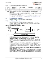
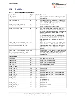
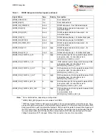
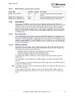
The MDDR is a hardened ASIC block for interfacing the DDR2, DDR3, and LPDDR1 memories. The
MDDR subsystem is used to access DDR memories for high-speed data transfers and code execution.,
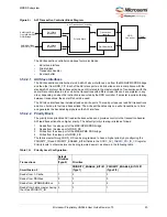
and includes a DDR memory controller, DDR PHY, and arbitration logic to support multiple masters. DDR
memory connected to the MDDR subsystem can be accessed by the MSS/HPMS masters and master
logic implemented in the FPGA fabric (FPGA fabric master).
The MSS/HPMS masters communicate with the MDDR subsystem through an MSS/HPMS DDR bridge
that provides an efficient access path. FPGA fabric masters communicate with the MDDR subsystem
through AXI or AHB interfaces.
3.1
Features
•
Integrated on-chip DDR memory controller and PHY
•
Capable of supporting LPDDR1, DDR2, and DDR3 memory devices
•
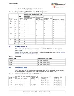
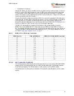
Up to 667 Mbps (333.33 MHz DDR) performance
•
Supports memory densities upto 4GB
•
Supports 8/16/32-bit DDR standard dynamic random access memory (SDRAM) data bus width
modes
•
Supports a maximum of 8 memory banks
•
Supports single rank memory
•
Single error correction and double error detection (SECDED) enable/disable feature
•
Supports DRAM burst lengths of 4, 8, or 16, depending on the bus-width mode and DDR type
configuration
•
Support for sequential and interleaved burst ordering
•
Programs internal control for ZQ short calibration cycles for DDR3 configurations
•
Supports dynamic scheduling to optimize bandwidth and latency
•
Supports self refresh entry and exit on command
•
Supports deep power-down entry and exit on command
•
Flexible address mapper logic to allow application specific mapping of row, column, bank, and rank
bits
•
Configurable support for 1T or 2T timing on the DDR SDRAM control signals
•
Supports autonomous DRAM power-down entry and exit caused by lack of transaction arrival for
programmable time
The following illustration shows the system level block diagram of the MDDR subsystem.


