Fabric DDR Subsystem
Microsemi ProprietaryUG0446 User Guide Revision 7.0
155
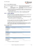
The DDR memories require delays after initializing the mode registers. The following registers must be
configured for delay requirements for the DDR memories. The DDR controller uses these delay values
while initializing the DDR memories.
•
DDRC_CKE_RSTN_CYCLES_1_CR (
page 73), recommended value is 0x4242
•
DDRC_ CKE_RSTN_CYCLES_2_CR (
page 74), recommended value is 0x8
4.6.10
Address Mapping
The DDR controller maps linear request addresses to DDR memory addresses by selecting the source
bit that maps to each and every applicable DDR memory address bit.
Each DDR memory address bit has an associated register vector to determine its source. The source
address bit number is determined by adding the internal base of a given register to the programmed
value for that register, as described in the following equation.
[Internal base] + [register value] = [source address bit number]
EQ 2
For example, reading the description for REG_DDRC_ADDRMAP_COL_B3, the internal base is 3; so
when the full data bus is in use, the column bit 4 is determined by 3 + [register value].
If this register is programmed to 2, then the source address bit is: 3 + 2 = 5.
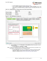
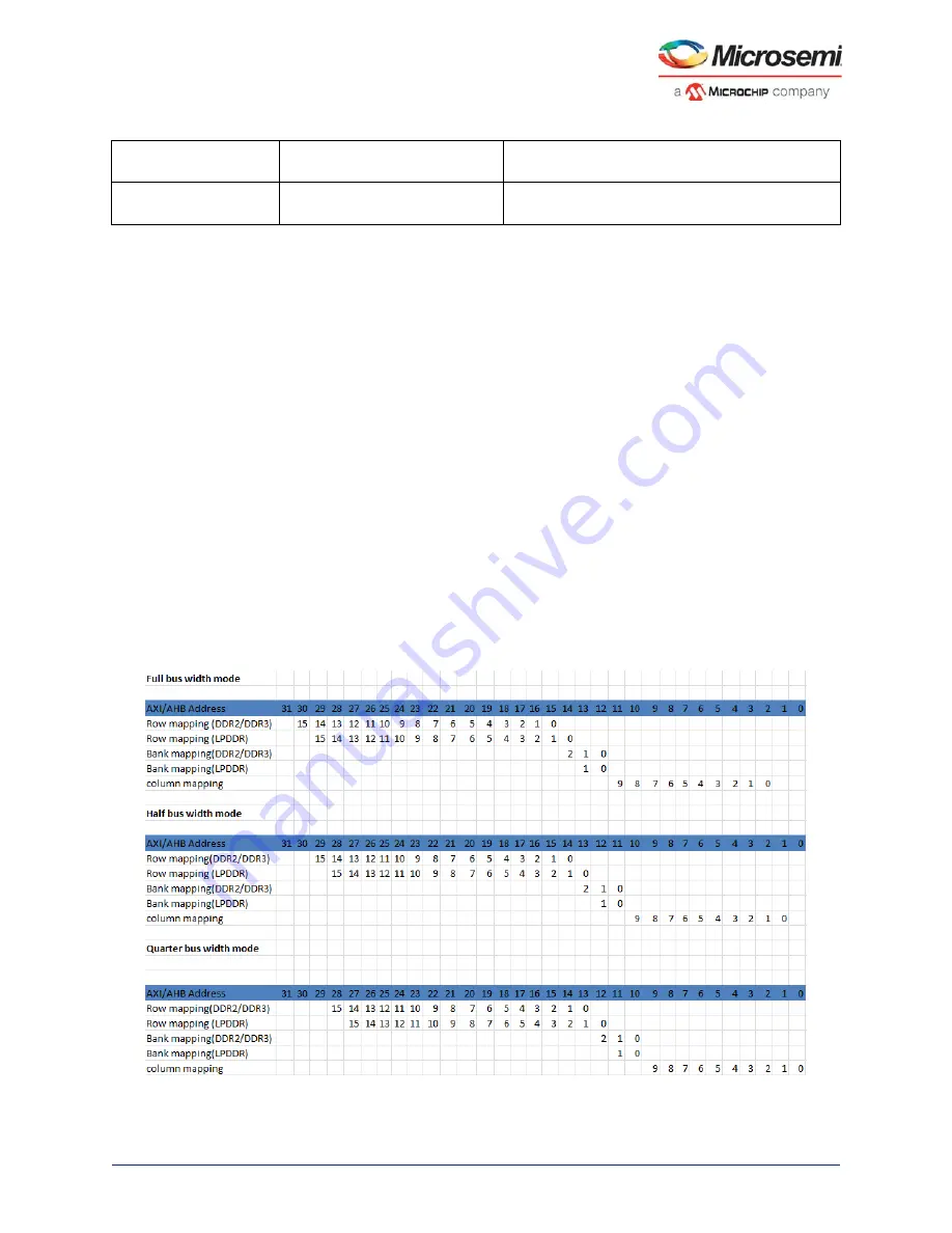
The DDR configurator assigns values to the address mapping registers depending on the selected
number of Columns, Rows and Banks. The following illustration provides the default mapping of the
memory row, bank, and column address to the user interface address domain.
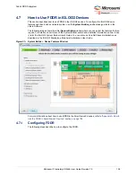
Figure 80 •
Address Mapping
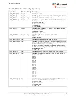
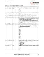
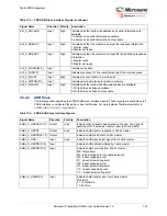
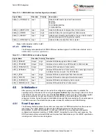
The following are the address mapping registers:
Write-to-read turnaround
time
REG_DDRC_WR2RD,
Minimum time to allow between issuing any Write
command and issuing any Read command
Write latency
REG_DDRC_WRITE_LATENCY,
Time after a Write command that write data should be
driven to DRAM.
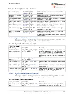
Table 138 •
Dynamic DRAM Global Constraints

