Fabric DDR Subsystem
Microsemi ProprietaryUG0446 User Guide Revision 7.0
199
8.
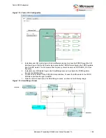
To verify the design in Libero SoC, create a SmartDesign testbench project and instantiate a DDR
memory model provided by the DDR memory vendor. Simulate the design and observe the AXI read
and write transactions.
Note:
The FDDR subsystem can be configured using the Cortex-M3 processor without having an APB master
in the FPGA fabric. The System Builder can be used to create the design by following steps in
. The System Builder provides "INIT_DONE" to indicate that the DDR
memory has been successfully initialized.
4.10.4
Use Model 2: Accessing FDDR from FPGA Fabric Through AHB
Interface
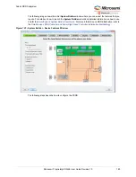
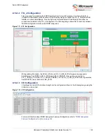
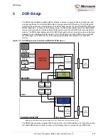
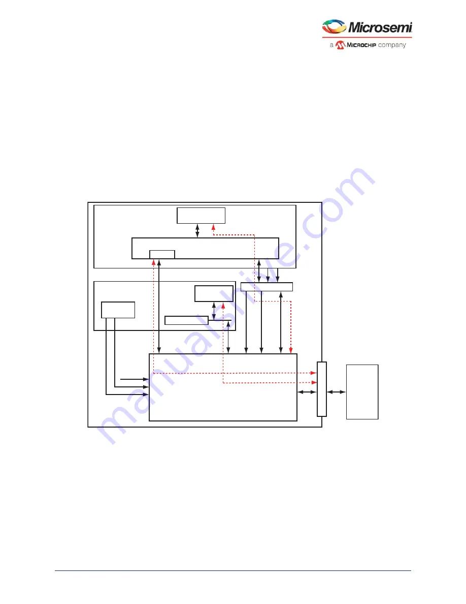
This use model shows an example of accessing DDR memory through the FDDR subsystem from two
AHB masters (refer to the following illustration). FIC_0 is used as AHB master 0 and user logic in the
fabric is used as AHB master 1. The FDDR registers are configured from the Cortex-M3 processor
through CoreConfigP. The read, write, and read-modify-write transactions are initiated by the AXI master
to read or write the data into the DDR memory after receiving the ready signal from the APB master.
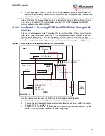
Figure 117 •
Accessing FDDR Subsystem Through Dual AHB Interface
Use the following steps to access the FDDR from the AXI master in the FPGA fabric:
1.
Instantiate the SmartFusion2 MSS component in the SmartDesign canvas.
2.
Configure the SmartFusion2 MSS peripheral components as required using the MSS configurator.
Configure FIC_0 as the AHB master.
3.
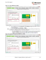
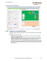
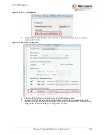
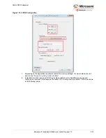
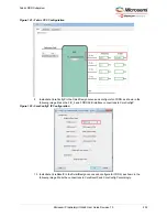
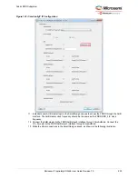
Configure FIC_2 to enable the FIC_2 APB interface for configuring the FDDR subsystem registers
from the Cortex-M3 processor, as shown in the following image.
ARM Cortex-M3
Processor
AHB Bus Matrix
MSS
FPGA Fabric
SmartFusion2
FDDR
FIC_0
FIC_2
FIC_2_APB_M_PRESET_N
FIC_2_APB_M_PCLK
APB_S_PCLK
APB_S_PRESET_N
APB_Slave
APB1_Slave
APB0_Slave
DDR
SDRAM
PADs
CCC
FAB_PLL_LOCK
CORE_RESET_N
CoreAHBLite
CoreSF2Config
AHB
Master
CLK_BASE
D
D
R
I
O

