DDR Bridge
Microsemi Proprietary UG0446 User Guide Revision 7.0
208
masters are fixed, as shown in the following table. The DDR bridges in the MDDR and FDDR
subsystems support only two AHB interfaces out of four and these can be used for user implemented
AHB masters.
Note:
If the AXI bus is selected as the interface between the FPGA fabric and the MDDR/ FDDR subsystem,
the DDR bridge in these subsystems is not used.
5.1
Functional Description
This section provides the detailed description of the DDR Bridge, which contains the following sections:
•
•
Details of Operation
5.1.1
Architecture Overview
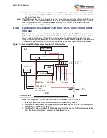
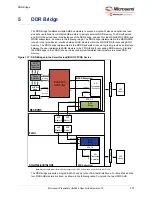
The DDR bridge consists of two main components: read and write combining buffers (WCB), and an
arbiter, as shown in the following illustration. The DDR bridge buffers AHB write transactions into write
combining buffers before bursting out to external DDR memory. It also includes read buffers for AHB
masters to efficiently read data from the external DDR memory. All buffers within the DDR bridge are
implemented with latches and hence are not subject to single event upsets (SEUs). The external DDR
memory regions can be configured to be non-bufferable. If a master interface requests a write or read to
a non-bufferable region, the DDR bridge is essentially bypassed. The size of the non-bufferable address
space can also be configured.
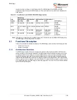
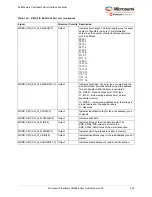
Table 163 •
SmartFusion2 and IGLOO2 FPGA DDR Bridge Interface
Sub-
System
DDR Bridge
AHB Interface 0
Read Only
AHB Interface 1
R/W
AHB Interface 2
R/W
AHB Interface 3
R/W
AXI Interface
HPMS
Not available—
Not available—
AHB bus matrix HPDMA
MDDR
subsystem
MSS
Cache Controller
IDC
Cache Controller
DS
AHB bus matrix HPDMA
MDDR
subsystem
MDDR
Not available
Not available
AHB master
interface 0
AHB master
interface 1
MDDR
subsystem
FDDR
Not available
Not available
AHB master
interface 0
AHB master
interface 1
FDDR
subsystem

