DDR Bridge
Microsemi Proprietary UG0446 User Guide Revision 7.0
213
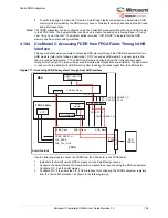
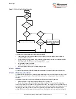
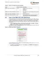
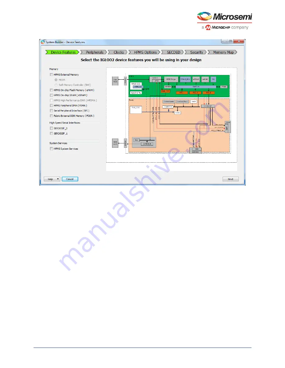
Figure 131 •
System Builder - Device Features Window
Navigate to the
HPMS Options
tab in the
System Builder
wizard.
For more information about how to use MDDR in the SmartFusion2 devices, refer to
Use DDR Bridge in SmartFusion2 Device" section on page 216
.
5.2.1
Configuring the DDR Bridge
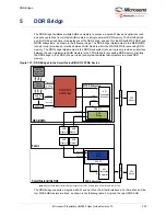
The following sections describe the configuration options for the HPMS DDR Bridge.
5.2.1.1
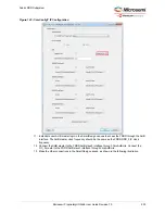
HPMS DDR Bridge Configurations
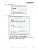
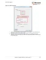
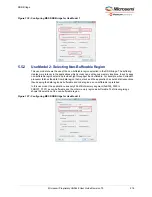
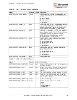
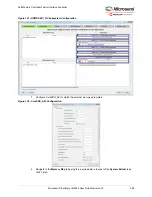
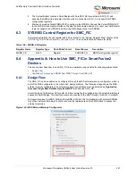
The HPMS DDR bridge is statically configured through the DDR bridge configurator in the System
Builder wizard. The following illustration shows the configuration options.
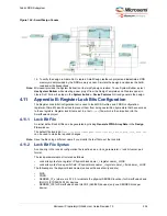
•
Write buffer time out counter
: This allows the user to configure the 10-bit timer of write buffer for
time out value. By default this is configured for maximum wait time (0×3FF) to buffer the write
transactions. For configuring to other values enter a 10-bit hexadecimal value in the provided field of
DDR bridge configurator. Select timeout value to a non zero value for buffering the write
transactions.
•
Non-bufferable region size
: The size of non-bufferable memory region can be selected from a
drop-down menu in the DDR bridge configurator. The menu has the options to select the region from
64 KB to 1 GB. It also has an option
None
to select the complete memory as bufferable. The default
selection is 64 KB.
•
Non-bufferable region address
: The base address of the non-bufferable memory region can be
selected by configuring this field. The value must be configured as a 16-bit hexadecimal address.
The default address is 0×A000. If the non-bufferable region size and address is left as default then
the 64 KB memory from 0×A0000000 address to 0×A0010000 address will be non-bufferable.
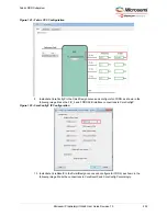
5. Enable or disable respective buffers allocated for each master. The selection of disabling the write/read buffer
makes all the transactions without buffering. By default buffering is enabled.Select the DDR burst size for

