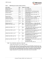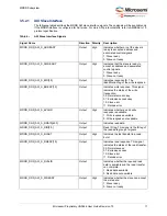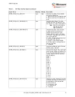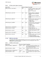
MDDR Subsystem
Microsemi Proprietary UG0446 User Guide Revision 7.0
18
3.5.3.4.2
Read Leveling
MDDR does not perform dynamic Read DQS Gate Training and Data Eye Training. Instead, these
functions are achieved by using built-in static delay values automatically generated by Libero SoC for the
MDDR automatic register initialization.
3.5.3.4.3
Read Gate
The DQS gate is aligned by the Libero SoC auto-generated MDDR initialization code containing fixed
delay ratios to account for board round-trip time between FPGA and the DDR3 memory. The
TMATCH_OUT and TMATCH_IN signals are shorted close to the FPGA balls to remove the FPGA
output and input delays from the round trip delay time. Therefore, the fixed delay ratios represent only the
board delay.
The fixed delay ratios work in combination with board layouts which follow the SmartFusion2/IGLOO2
Board Design Guidelines (refer
AC393: Board Design Guidelines for SmartFusion2/IGLOO2 FPGA
).
3.5.3.4.4
DQS Alignment within Data Eye
The incoming read DQS is internally centered within the read DQ data window using a static delay ratio.
This static delay is applied by the Libero SoC auto-generated MDDR initialization code. The fixed delay
ratios work in combination with board layouts which follow the SmartFusion2/IGLOO2 Board Design
Guidelines (refer
AC393: Board Design Guidelines for SmartFusion2/IGLOO2 FPGA Application Note
Note:
The Libero SOC auto-generated delay ratio for read DQS data eye centering is written to the required
register.
3.5.3.5
DDR Memory Initialization Time
The time to initialize the DDR memory depends on the following factors:
•
Power-up and register initialization by system controller. It depends on the power on reset delay
configuration in the Libero project (
Project
>
Project Settings
>
Device settings
).
•
DDR controller and PHY configuration registers initialization. In SmartFusion2 devices, the Cortex-
M3 initializes these registers. In IGLOO2 devices, the ConfigMaster in the FPGA fabric initializes
these registers.
•
DDR memory initialization by the DDR Controller according to the JEDEC standard (mode register
configuration and training).
•
DDR memory settling time configured in the System Builder memory configuration window.
3.5.4
Details of Operation
This section provides a functional description of each block in the MDDR subsystem.
3.5.4.1
DDR_FIC
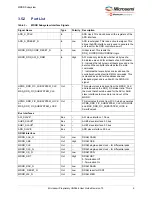
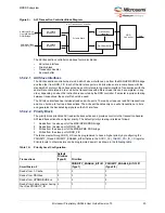
The following illustration shows the DDR_FIC block diagram.
Figure 4 •
DDR_FIC Block Diagram
Fabric masters can access the MDDR subsystem in the following ways:
•
Single AXI-64 interface
•
Single AHB-32 interface
Configuration
Registers
16-Bit APB
Configuration Bus
64-Bit AXI / Single
32-Bit AHBL /
Dual 32-Bit AHBL
Slave Interface
MUX
DDR Bridge
AXI-AXI
Synchronous
Bridge
MUX
AHB
AHB
AXI
AXI
AXI
AXI Transaction
Controller


