MDDR Subsystem
Microsemi Proprietary UG0446 User Guide Revision 7.0
61
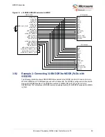
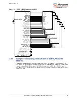
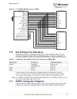
Figure 45 •
×16 LPDDR1 SDRAM Connection to MDDR
3.10
Board Design Considerations
MDDR/FDDR subsystems are interfaced with DDR memories through DDRIO. DDRIO is a multi-
standard IO optimized for LPDDR, DDR2, and DDR3 performance. The following table lists the IO
standards and calibration resistance requirements for MDDR/FDDR to interface with DDR memories.
For more information on IO Standards and Calibration Resistance Requirements, refer to the
AC394: Layout Guidelines for SmartFusion2/IGLOO2-Based Board Design Application Note
AC393: Board Design Guidelines for SmartFusion2 SoC and IGLOO2 FPGA Application Note
.
Note:
For LVCMOS18 IO Standard, the user can optionally calibrate the IO. If calibration is desired, the user
must install the appropriate resistor on the PCB.
3.11
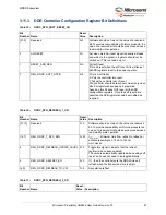
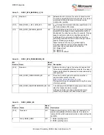
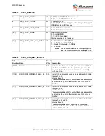
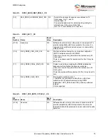
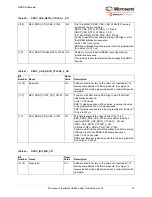
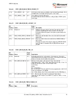
MDDR Configuration Registers
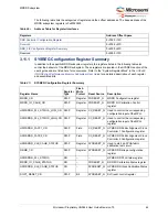
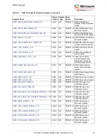
This section provides MDDR subsystem registers along with the address offset, functionality, and bit
definitions. The registers are categorized based on the controller blocks in the MDDR subsystem.
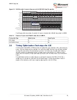
Table 25 •
I/O Standards and Calibration Resistance Requirements for MDDR/FDDR
Memory Type
IO Standard
Calibration Resistor
LPDDR
LVCMOS18
LPDDRI(SSTL18)
Not Required*
Required
DDR2
SSTL18
Required
DDR3
SSTL15
Required
CASN
CKE
CLK_P
CLK_N
CSN
RASN
WEN
ADDR[12:0]
BA[2:0]
MT46H32M16LF
MDDR_CAS_N
MDDR_CKE
MDDR_CLK
MDDR_CLK_N
MDDR_CS_N
MDDR_RAS_N
MDDR_WE_N
MDDR_ADDR[12:0]
MDDR_BA[1:0]
MDDR_DM_RDQS[1:0]
MDDR_DQS[0]
MDDR_DQ[15:0]
DQ[15:0]
UDQS
LDQS
UDM, LDM
CASN
CKE
CLK_P
CLK_N
CSN
RASN
WEN
ADDR[12:0]
BA[2:0]
MT46H32M16LF
DQ[1:0]
LDQS
LDM
MDDR_DM_RDQS_ECC
MDDR_DQS_ECC
MDDR_DQ_ECC[1:0]
MDDR_DQS[1]
MDDR_PADS
MDDR_DQS_TMATCH_0_IN
MDDR_DQS_TMATCH_0_OUT
MDDR_IMP_CALIB
R
MDDR_DQS_TMATCH_ECC_IN
MDDR_DQS_TMATCH_ECC_OUT


