PIC16C62B/72A
DS35008C-page 100
Preliminary
1998-2013 Microchip Technology Inc.
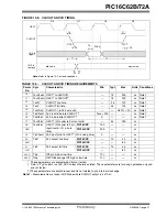
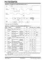
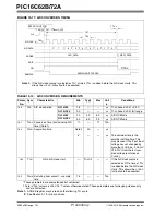
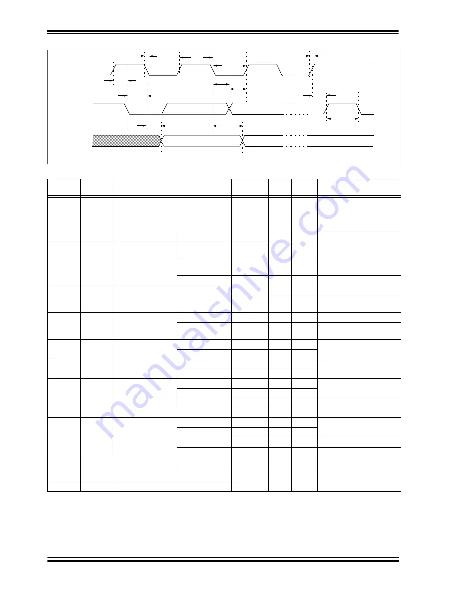
FIGURE 13-16: I
2
C BUS DATA TIMING
TABLE 13-12: I
2
C BUS DATA REQUIREMENTS
Param.
No.
Sym
Characteristic
Min
Max
Units
Conditions
100*
T
HIGH
Clock high time
100 kHz mode
4.0
—
s
Device must operate at a min-
imum of 1.5 MHz
400 kHz mode
0.6
—
s
Device must operate at a min-
imum of 10 MHz
SSP Module
1.5T
CY
—
101*
T
LOW
Clock low time
100 kHz mode
4.7
—
s
Device must operate at a min-
imum of 1.5 MHz
400 kHz mode
1.3
—
s
Device must operate at a min-
imum of 10 MHz
SSP Module
1.5T
CY
—
102*
T
R
SDA and SCL rise
time
100 kHz mode
—
1000
ns
400 kHz mode
20 + 0.1Cb
300
ns
Cb is specified to be from
10-400 pF
103*
T
F
SDA and SCL fall
time
100 kHz mode
—
300
ns
400 kHz mode
20 + 0.1Cb
300
ns
Cb is specified to be from
10-400 pF
90*
T
SU
:
STA
START condition
setup time
100 kHz mode
4.7
—
s
Only relevant for repeated
START condition
400 kHz mode
0.6
—
s
91*
T
HD
:
STA
START condition hold
time
100 kHz mode
4.0
—
s
After this period the first clock
pulse is generated
400 kHz mode
0.6
—
s
106*
T
HD
:
DAT
Data input hold time
100 kHz mode
0
—
ns
400 kHz mode
0
0.9
s
107*
T
SU
:
DAT
Data input setup time
100 kHz mode
250
—
ns
Note 2
400 kHz mode
100
—
ns
92*
T
SU
:
STO
STOP condition setup
time
100 kHz mode
4.7
—
s
400 kHz mode
0.6
—
s
109*
T
AA
Output valid from
clock
100 kHz mode
—
3500
ns
Note 1
400 kHz mode
—
—
ns
110*
T
BUF
Bus free time
100 kHz mode
4.7
—
s
Time the bus must be free
before a new transmission
can start
400 kHz mode
1.3
—
s
Cb
Bus capacitive loading
—
400
pF
*
These parameters are characterized but not tested.
Note 1:
As a transmitter, the device must provide this internal minimum delay time to bridge the undefined region (min. 300 ns) of the fall-
ing edge of SCL to avoid unintended generation of START or STOP conditions.
2:
A fast-mode (400 kHz) I
2
C-bus device can be used in a standard-mode (100 kHz) I
2
C-bus system, but the requirement Tsu:DAT
250 ns must then be met. This will automatically be the case if the device does not stretch the LOW period of the SCL signal. If
such a device does stretch the LOW period of the SCL signal, it must output the next data bit to the SDA line T
R
max.+tsu;DAT = 1000 + 250 = 1250 ns (according to the standard-mode I
2
C bus specification) before the SCL line is released.
Note:
Refer to Figure 13-4 for load conditions.
90
91
92
100
101
103
106
107
109
109
110
102
SCL
SDA
In
SDA
Out
Summary of Contents for PIC16C62B/72A
Page 4: ...PIC16C62B 72A DS35008C page 4 Preliminary 1998 2013 Microchip Technology Inc NOTES...
Page 30: ...PIC16C62B 72A DS35008C page 30 Preliminary 1998 2013 Microchip Technology Inc NOTES...
Page 38: ...PIC16C62B 72A DS35008C page 38 Preliminary 1998 2013 Microchip Technology Inc NOTES...
Page 48: ...PIC16C62B 72A DS35008C page 48 Preliminary 1998 2013 Microchip Technology Inc NOTES...
Page 80: ...PIC16C62B 72A DS35008C page 80 Preliminary 1998 2013 Microchip Technology Inc NOTES...
Page 104: ...PIC16C62B 72A DS35008C page 104 Preliminary 1998 2013 Microchip Technology Inc NOTES...
Page 110: ...PIC16C62B 72A DS35008C page 110 Preliminary 1998 2013 Microchip Technology Inc NOTES...
Page 120: ...PIC16C62B 72A DS35008C page 120 Preliminary 1913 Microchip Technology Inc...

