PIC16C62B/72A
1998-2013 Microchip Technology Inc.
Preliminary
DS35008C-page 53
9.2
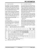
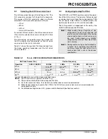
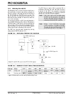
Selecting the A/D Conversion Clock
The A/D conversion time per bit is defined as T
AD
. The
A/D conversion requires 9.5T
AD
per 8-bit conversion.
The source of the A/D conversion clock is software
selectable. The four possible options for T
AD
are:
• 2T
OSC
• 8T
OSC
• 32T
OSC
• Internal RC oscillator
For correct A/D conversions, the A/D conversion clock
(T
AD
) must be selected to ensure a minimum T
AD
time
of 1.6
s.
The A/D module can operate during sleep mode, but
the RC oscillator must be selected as the A/D clock
source prior to the
SLEEP
instruction.
Table 9-1 shows the resultant T
AD
times derived from
the device operating frequencies and the A/D clock
source selected.
9.3
Configuring Analog Port Pins
The ADCON1 and TRISA registers control the opera-
tion of the A/D port pins. The port pins that are desired
as analog inputs must have their corresponding TRIS
bits set (input). If the TRIS bit is cleared (output), the
digital output level (V
OH
or V
OL
) will be converted.
The A/D operation is independent of the state of the
CHS2:CHS0 bits and the TRIS bits.
TABLE 9-1
T
AD
vs. DEVICE OPERATING FREQUENCIES
Note 1:
When reading the port register, all pins
configured as analog input channels will
read as cleared (a low level). Pins config-
ured as digital inputs, will convert an ana-
log input. Analog levels on a digitally
configured input will not affect the conver-
sion accuracy.
Note 2:
Analog levels on any pin that is defined as
a digital input (including the AN4:AN0
pins) may cause the input buffer to con-
sume current that is out of the devices
specification.
AD Clock Source (T
AD
)
Device Frequency
Operation
ADCS1:ADCS0
20 MHz
5 MHz
1.25 MHz
333.33 kHz
2T
OSC
00
100 ns
(2)
400 ns
(2)
1.6
s
6
s
8T
OSC
01
400 ns
(2)
1.6
s
6.4
s
24
s
(3)
32T
OSC
10
1.6
s
6.4
s
25.6
s
(3)
96
s
(3)
RC
(5)
11
2 - 6
s
(1,4)
2 - 6
s
(1,4)
2 - 6
s
(1,4)
2 - 6
s
(1)
Legend: Shaded cells are outside of recommended range.
Note 1:
The RC source has a typical T
AD
time of 4
s.
2:
These values violate the minimum required T
AD
time.
3:
For faster conversion times, the selection of another clock source is recommended.
4:
When device frequency is greater than 1 MHz, the RC A/D conversion clock source is recommended for
sleep operation only.
5:
For extended voltage devices (LC), please refer to Electrical Specifications section.
Summary of Contents for PIC16C62B/72A
Page 4: ...PIC16C62B 72A DS35008C page 4 Preliminary 1998 2013 Microchip Technology Inc NOTES...
Page 30: ...PIC16C62B 72A DS35008C page 30 Preliminary 1998 2013 Microchip Technology Inc NOTES...
Page 38: ...PIC16C62B 72A DS35008C page 38 Preliminary 1998 2013 Microchip Technology Inc NOTES...
Page 48: ...PIC16C62B 72A DS35008C page 48 Preliminary 1998 2013 Microchip Technology Inc NOTES...
Page 80: ...PIC16C62B 72A DS35008C page 80 Preliminary 1998 2013 Microchip Technology Inc NOTES...
Page 104: ...PIC16C62B 72A DS35008C page 104 Preliminary 1998 2013 Microchip Technology Inc NOTES...
Page 110: ...PIC16C62B 72A DS35008C page 110 Preliminary 1998 2013 Microchip Technology Inc NOTES...
Page 120: ...PIC16C62B 72A DS35008C page 120 Preliminary 1913 Microchip Technology Inc...

