background image

 2000 Microchip Technology Inc.

DS30605C-page 175

PIC16C63A/65B/73B/74B

ON-LINE SUPPORT

Microchip provides on-line support on the Microchip
World Wide Web (WWW) site.

The web site is used by Microchip as a means to make
files and information easily available to customers. To
view the site, the user must have access to the Internet
and a web browser, such as Netscape or Microsoft
Explorer. Files are also available for FTP download
from our FTP site.

Connecting to the Microchip Internet Web Site      

The Microchip web site is available by using your
favorite Internet browser to attach to: 

www.microchip.com

The file transfer site is available by using an FTP ser-
vice to connect to: 

ftp://ftp.microchip.com

The web site and file transfer site provide a variety of
services. Users may download files for the latest
Development Tools, Data Sheets, Application Notes,
User’s Guides, Articles and Sample Programs. A vari-
ety of Microchip specific business information is also
available, including listings of Microchip sales offices,
distributors and factory representatives. Other data
available for consideration is:

• Latest Microchip Press Releases

• Technical Support Section with Frequently Asked 

Questions 

• Design Tips

• Device Errata

• Job Postings

• Microchip Consultant Program Member Listing

• Links to other useful web sites related to 

Microchip Products

• Conferences for products, Development Systems, 

technical information and more

• Listing of seminars and events

Systems Information and Upgrade Hot Line 

The Systems Information and Upgrade Line provides
system users a listing of the latest versions of all of
Microchip's development systems software products.
Plus, this line provides information on how customers
can receive any currently available upgrade kits.The
Hot Line Numbers are: 

1-800-755-2345 for U.S. and most of Canada, and 

1-480-792-7302 for the rest of the world.

Trademarks: The Microchip name, logo, PIC, PICmicro, 
PICMASTER, PICSTART, PRO MATE, K

EE

L

OQ

, SEEVAL, 

MPLAB and The Embedded Control Solutions Company 
are registered trademarks of Microchip Technology 
Incorporated in the U.S.A. and other countries.  
Total Endurance, ICSP, In-Circuit Serial Programming, 
FilterLab, MXDEV, microID, FlexROM, fuzzyLAB, MPASM, 
MPLINK, MPLIB, PICDEM, ICEPIC and Migratable 
Memory are trademarks and SQTP is a service mark of 
Microchip in the U.S.A. 

All other trademarks mentioned herein are the property of 
their respective companies.

001024

Summary of Contents for PIC16C63A

Page 1: ... timer counter with prescaler can be incremented during SLEEP via external crystal clock Timer2 8 bit timer counter with 8 bit period register prescaler and postscaler Capture Compare PWM modules Capture is 16 bit max resolution is 200 ns Compare is 16 bit max resolution is 200 ns PWM max resolution is 10 bit 8 bit multichannel Analog to Digital converter Synchronous Serial Port SSP with SPITM and...

Page 2: ...RA5 SS AN4 RA4 T0CKI RC7 RX DT RD4 PSP4 RD5 PSP5 RD6 PSP6 RD7 PSP7 VSS VDD RB0 INT RB1 RB2 RB3 RC6 TX CK RC5 SDO RC4 SDI SDA RD3 PSP3 RD2 PSP2 RD1 PSP1 RD0 PSP0 RC3 SCK SCL RC2 CCP1 RC1 T1OSI CCP2 NC 1 2 3 4 5 6 7 8 9 10 11 33 32 31 30 29 28 27 26 25 24 23 RA3 AN3 V REF RA2 AN2 RA1 AN1 RA0 AN0 MCLR V PP RB7 RB6 RB5 RB4 NC NC 44 43 42 41 40 39 38 37 36 35 34 22 21 20 19 18 17 16 15 14 13 12 MQFP PL...

Page 3: ...ou have any questions or comments regarding this publication please contact the Marketing Communications Department via E mail at docerrors mail microchip com or fax the Reader Response Form in the back of this data sheet to 480 792 4150 We welcome your feedback Most Current Data Sheet To obtain the most up to date version of this data sheet please register at our Worldwide Web site at http www mi...

Page 4: ...PIC16C63A 65B 73B 74B DS30605C page 4 2000 Microchip Technology Inc NOTES ...

Page 5: ...ing system reliability and reducing power consumption There are four oscillator options of which the single pin RC oscillator provides a low cost solution the LP oscillator minimizes power consumption XT is a standard crystal and the HS is for high speed crys tals The SLEEP power down feature provides a power saving mode The user can wake up the chip from SLEEP through several external and interna...

Page 6: ...PIC16C63A 65B 73B 74B DS30605C page 6 2000 Microchip Technology Inc NOTES ...

Page 7: ...2 One Time Programmable OTP Devices The availability of OTP devices is especially useful for customers who need the flexibility for frequent code updates and small volume applications The OTP devices packaged in plastic packages per mit the user to program them once In addition to the program memory the configuration bits must also be programmed 2 3 Quick Turnaround Production QTP Devices Microchi...

Page 8: ...PIC16C63A 65B 73B 74B DS30605C page 8 2000 Microchip Technology Inc NOTES ...

Page 9: ...Reg isters including the program counter are mapped in the data memory The PIC16CXX has an orthogonal symmetrical instruction set that makes it possible to carry out any operation on any register using any addressing mode This symmetrical nature and lack of special optimal situations make programming with the PIC16CXX simple yet efficient In addition the learning curve is reduced significantly PIC...

Page 10: ...on OSC1 CLKIN OSC2 CLKOUT MCLR VDD VSS PORTA PORTB PORTC PORTD 3 PORTE 3 RA4 T0CKI RA5 SS AN4 2 RB0 INT RB7 RB1 RC0 T1OSO T1CKI RC1 T1OSI CCP2 RC2 CCP1 RC3 SCK SCL RC4 SDI SDA RC5 SDO RC6 TX CK RC7 RX DT RD6 PSP6 RE0 RD AN5 2 3 RE1 WR AN6 2 3 RE2 CS AN7 2 3 8 8 Brown out Reset Note 1 Higher order bits are from the STATUS register 2 A D is not available on the PIC16C63A 65B 3 PSP and Ports D and E ...

Page 11: ...RB4 25 25 I O TTL Interrupt on change pin RB5 26 26 I O TTL Interrupt on change pin RB6 27 27 I O TTL ST 2 Interrupt on change pin Serial programming clock RB7 28 28 I O TTL ST 2 Interrupt on change pin Serial programming data PORTC is a bi directional I O port RC0 T1OSO T1CKI 11 11 I O ST RC0 can also be the Timer1 oscillator output or Timer1 clock input RC1 T1OSI CCP2 12 12 I O ST RC1 can also b...

Page 12: ...put is open drain type RA5 SS AN4 5 7 8 24 I O TTL RA5 can also be analog input 4 5 or the slave select for the synchronous serial port PORTB is a bi directional I O port PORTB can be software programmed for internal weak pull up on all inputs RB0 INT 33 36 8 I O TTL ST 1 RB0 can also be the external interrupt pin RB1 34 37 9 I O TTL RB2 35 38 10 I O TTL RB3 36 39 11 I O TTL RB4 37 41 14 I O TTL I...

Page 13: ...29 32 4 I O ST TTL 3 RD7 PSP7 30 33 5 I O ST TTL 3 PORTE is a bi directional I O port RE0 RD AN5 5 8 9 25 I O ST TTL 3 RE0 can also be read control for the parallel slave port or analog input 5 5 RE1 WR AN6 5 9 10 26 I O ST TTL 3 RE1 can also be write control for the parallel slave port or analog input 6 5 RE2 CS AN7 5 10 11 27 I O ST TTL 3 RE2 can also be select control for the parallel slave por...

Page 14: ... g GOTO then two cycles are required to complete the instruction Example 3 1 A fetch cycle begins with the program counter PC incrementing in Q1 In the execution cycle the fetched instruction is latched into the Instruction Register IR in cycle Q1 This instruction is then decoded and executed during the Q2 Q3 and Q4 cycles Data memory is read during Q2 operand read and written during Q4 destinatio...

Page 15: ...gisters GPR and the Special Function Registers SFR Bits RP1 and RP0 are the bank select bits RP1 RP0 STATUS 6 5 00 Bank0 01 Bank1 10 Bank2 11 Bank3 Each bank extends up to 7Fh 128 bytes The lower locations of each bank are reserved for the SFRs Above the SFRs are GPRs implemented as static RAM All implemented banks contain SFRs Frequently used SFRs from one bank may be mirrored in another bank for...

Page 16: ... PCLATH INTCON PIR1 PIR2 TMR1L TMR1H T1CON TMR2 T2CON SSPBUF SSPCON CCPR1L CCPR1H CCP1CON RCSTA TXREG RCREG CCPR2L CCPR2H CCP2CON ADRES 3 ADCON0 3 INDF 1 OPTION_REG PCL STATUS FSR TRISA TRISB TRISC TRISD 2 TRISE 2 PCLATH INTCON PIE1 PIE2 PCON PR2 SSPADD SSPSTAT TXSTA SPBRG ADCON1 3 00h 01h 02h 03h 04h 05h 06h 07h 08h 09h 0Ah 0Bh 0Ch 0Dh 0Eh 0Fh 10h 11h 12h 13h 14h 15h 16h 17h 18h 19h 1Ah 1Bh 1Ch 1...

Page 17: ...000 uu uuuu 11h TMR2 Timer2 module s register 0000 0000 0000 0000 12h T2CON TOUTPS3 TOUTPS2 TOUTPS1 TOUTPS0 TMR2ON T2CKPS1 T2CKPS0 000 0000 000 0000 13h SSPBUF Synchronous Serial Port Receive Buffer Transmit Register xxxx xxxx uuuu uuuu 14h SSPCON WCOL SSPOV SSPEN CKP SSPM3 SSPM2 SSPM1 SSPM0 0000 0000 0000 0000 15h CCPR1L Capture Compare PWM Register1 LSB xxxx xxxx uuuu uuuu 16h CCPR1H Capture Com...

Page 18: ...ed 92h PR2 Timer2 Period register 1111 1111 1111 1111 93h SSPADD Synchronous Serial Port I2 C mode Address register 0000 0000 0000 0000 94h SSPSTAT D A P S R W UA BF 00 0000 00 0000 95h Unimplemented 96h Unimplemented 97h Unimplemented 98h TXSTA CSRC TX9 TXEN SYNC BRGH TRMT TX9D 0000 010 0000 010 99h SPBRG Baud Rate Generator register 0000 0000 0000 0000 9Ah Unimplemented 9Bh Unimplemented 9Ch Uni...

Page 19: ...F instruc tions for examples R W 0 R W 0 R W 0 R 1 R 1 R W x R W x R W x IRP 1 RP1 1 RP0 TO PD Z DC C 2 bit 7 bit 0 bit 7 IRP 1 Register Bank Select bit used for indirect addressing 1 Bank 2 3 100h 1FFh 0 Bank 0 1 00h FFh bit 6 5 RP1 1 RP0 Register Bank Select bits used for direct addressing 11 Bank 3 180h 1FFh 10 Bank 2 100h 17Fh 01 Bank 1 80h FFh 00 Bank 0 00h 7Fh Each bank is 128 bytes bit 4 TO...

Page 20: ... individual port latch values bit 6 INTEDG Interrupt Edge Select bit 1 Interrupt on rising edge of RB0 INT pin 0 Interrupt on falling edge of RB0 INT pin bit 5 T0CS TMR0 Clock Source Select bit 1 Transition on RA4 T0CKI pin 0 Internal instruction cycle clock CLKOUT bit 4 T0SE TMR0 Source Edge Select bit 1 Increment on high to low transition on RA4 T0CKI pin 0 Increment on low to high transition on...

Page 21: ...Disables all peripheral interrupts bit 5 T0IE TMR0 Overflow Interrupt Enable bit 1 Enables the TMR0 interrupt 0 Disables the TMR0 interrupt bit 4 INTE RB0 INT External Interrupt Enable bit 1 Enables the RB0 INT external interrupt 0 Disables the RB0 INT external interrupt bit 3 RBIE RB Port Change Interrupt Enable bit 1 Enables the RB port change interrupt 0 Disables the RB port change interrupt bi...

Page 22: ...SART receive interrupt bit 4 TXIE USART Transmit Interrupt Enable bit 1 Enables the USART transmit interrupt 0 Disables the USART transmit interrupt bit 3 SSPIE Synchronous Serial Port Interrupt Enable bit 1 Enables the SSP interrupt 0 Disables the SSP interrupt bit 2 CCP1IE CCP1 Interrupt Enable bit 1 Enables the CCP1 interrupt 0 Disables the CCP1 interrupt bit 1 TMR2IE TMR2 to PR2 Match Interrup...

Page 23: ...mpty bit 4 TXIF USART Transmit Interrupt Flag bit 1 The USART transmit buffer is empty clear by writing to TXREG 0 The USART transmit buffer is full bit 3 SSPIF Synchronous Serial Port Interrupt Flag bit 1 The transmission reception is complete must be cleared in software 0 Waiting to transmit receive bit 2 CCP1IF CCP1 Interrupt Flag bit Capture mode 1 A TMR1 register capture occurred must be clea...

Page 24: ...0 Bit is cleared x Bit is unknown Note Interrupt flag bits are set when an interrupt condition occurs regardless of the state of its corresponding enable bit or the global enable bit GIE INTCON 7 User soft ware should ensure the appropriate inter rupt flag bits are clear prior to enabling an interrupt U 0 U 0 U 0 U 0 U 0 U 0 U 0 R W 0 CCP2IF bit 7 bit 0 bit 7 1 Unimplemented Read as 0 bit 0 CCP2IF...

Page 25: ...BOR status bit is a don t care and is not predictable if the brown out circuit is disabled by clear ing the BODEN bit in the configuration word U 0 U 0 U 0 U 0 U 0 U 0 R W 0 R W q POR BOR bit 7 bit 0 bit 7 2 Unimplemented Read as 0 bit 1 POR Power on Reset Status bit 1 No Power on Reset occurred 0 A Power on Reset occurred must be set in software after a Power on Reset occurs bit 0 BOR Brown out R...

Page 26: ...ssing a contin uous 8K word block of program memory The CALL and GOTO instructions provide only 11 bits of address to allow branching within any 2K program memory page When executing a CALL or GOTO instruction the upper 2 bits of the address are provided by PCLATH 4 3 When doing a CALL or GOTO instruction the user must ensure that the page select bits are programmed so that the desired program mem...

Page 27: ...ng the 8 bit FSR register and the IRP bit STATUS 7 as shown in Figure 4 4 A simple program to clear RAM locations 20h 2Fh using indirect addressing is shown in Example 4 2 EXAMPLE 4 2 INDIRECT ADDRESSING movlw 0x20 initialize pointer movwf FSR to RAM NEXT clrf INDF clear INDF register incf FSR F inc pointer btfss FSR 4 all done goto NEXT no clear next CONTINUE yes continue FIGURE 4 4 DIRECT INDIRE...

Page 28: ...PIC16C63A 65B 73B 74B DS30605C page 28 2000 Microchip Technology Inc NOTES ...

Page 29: ...PIC16C73B 74B PORTA pins are multiplexed with analog inputs and analog VREF input The opera tion of each pin is selected by clearing setting the con trol bits in the ADCON1 register A D Control Register1 The TRISA register controls the direction of the RA pins even when they are being used as analog inputs The user must ensure the bits in the TRISA register are maintained set when using them as an...

Page 30: ...lave select input for synchronous serial port or analog input Legend TTL TTL input ST Schmitt Trigger input Note 1 The A D is not implemented on the PIC16C63A 65B Pins will operate as digital I O only ADCON1 is not implemented maintain this register clear Address Name Bit 7 Bit 6 Bit 5 Bit 4 Bit 3 Bit 2 Bit 1 Bit 0 Value on POR BOR Value on all other RESETS 05h PORTA RA5 RA4 RA3 RA2 RA1 RA0 0x 000...

Page 31: ... Clear flag bit RBIF A mismatch condition will continue to set flag bit RBIF Reading PORTB will end the mismatch condition and allow flag bit RBIF to be cleared This interrupt on mismatch feature together with soft ware configurable pull ups on these four pins allow easy interface to a keypad and make it possible for wake up on key depression Refer to the Embedded Control Handbook Implementing Wak...

Page 32: ...l software programmable weak pull up RB6 bit6 TTL ST 2 Input output pin with interrupt on change Internal software programmable weak pull up Serial programming clock RB7 bit7 TTL ST 2 Input output pin with interrupt on change Internal software programmable weak pull up Serial programming data Legend TTL TTL input ST Schmitt Trigger input Note 1 This buffer is a Schmitt Trigger input when configure...

Page 33: ...eral OE 3 Peripheral Input I O pin 1 Note 1 I O pins have diode protection to VDD and VSS 2 Port Peripheral select signal selects between port data and peripheral output 3 Peripheral OE output enable is only activated if peripheral select is active Name Bit Buffer Type Function RC0 T1OSO T1CKI bit0 ST Input output port pin or Timer1 oscillator output Timer1 clock input RC1 T1OSI CCP2 bit1 ST Input...

Page 34: ... port bit0 RD1 PSP1 bit1 ST TTL 1 Input output port pin or parallel slave port bit1 RD2 PSP2 bit2 ST TTL 1 Input output port pin or parallel slave port bit2 RD3 PSP3 bit3 ST TTL 1 Input output port pin or parallel slave port bit3 RD4 PSP4 bit4 ST TTL 1 Input output port pin or parallel slave port bit4 RD5 PSP5 bit5 ST TTL 1 Input output port pin or parallel slave port bit5 RD6 PSP6 bit6 ST TTL 1 I...

Page 35: ...RAM TABLE 5 9 PORTE FUNCTIONS Note 1 The PIC16C63A and PIC16C73B do not provide PORTE The PORTE and TRISE registers are not implemented 2 The PIC16C63A 65B does not provide an A D module A D functions are not imple mented Note On a Power on Reset these pins are con figured as analog inputs and read as 0 s Data Bus WR Port WR TRIS RD Port Data Latch TRIS Latch RD TRIS Schmitt Trigger Input Buffer Q...

Page 36: ...st be cleared in software 0 No overflow occurred bit 4 PSPMODE Parallel Slave Port Mode Select bit 1 Parallel Slave Port mode 0 General purpose I O mode bit 3 Unimplemented Read as 0 bit 2 TRISE2 Direction Control bit for pin RE2 CS AN7 1 Input 0 Output bit 1 TRISE1 Direction Control bit for pin RE1 WR AN6 1 Input 0 Output bit 0 TRISE0 Direction Control bit for pin RE0 RD AN5 1 Input 0 Output Lege...

Page 37: ... on the Q4 clock cycle following the next Q2 cycle to signal the write is complete Figure 5 9 The interrupt flag bit PSPIF PIR1 7 is also set on the same Q4 clock cycle IBF can only be cleared by reading the PORTD input latch The Input Buffer Overflow IBOV status flag bit TRISE 5 is set if a second write to the PSP is attempted when the previous byte has not been read out of the buffer A read from...

Page 38: ...Bit 1 Bit 0 Value on POR BOR Value on all other RESETS 08h PORTD Port data latch when written Port pins when read xxxx xxxx uuuu uuuu 09h PORTE RE2 RE1 RE0 xxx uuu 0Bh 8Bh INTCON GIE PEIE T0IE INTE RBIE T0IF INTF RBIF 0000 000x 0000 000u 89h TRISE IBF OBF IBOV PSPMODE PORTE Data Direction Bits 0000 111 0000 111 0Ch PIR1 PSPIF ADIF RCIF TXIF SSPIF CCP1IF TMR2IF TMR1IF 0000 0000 0000 0000 8Ch PIE1 P...

Page 39: ... falling edge of pin RA4 T0CKI The incrementing edge is determined by the Timer0 Source Edge Select bit T0SE OPTION_REG 4 Clearing bit T0SE selects the ris ing edge Restrictions on the external clock input are discussed in detail in Section 6 2 The prescaler is mutually exclusively shared between the Timer0 module and the watchdog timer The prescaler is not readable or writable Section 6 3 details...

Page 40: ... the Watchdog Timer The prescaler is not readable or writable REGISTER 6 1 OPTION_REG REGISTER Note Writing to TMR0 when the prescaler is assigned to Timer0 will clear the prescaler count but will not change the prescaler assignment R W 1 R W 1 R W 1 R W 1 R W 1 R W 1 R W 1 R W 1 RBPU INTEDG T0CS T0SE PSA PS2 PS1 PS0 bit 7 bit 0 bit 7 RBPU bit 6 INTEDG bit 5 T0CS TMR0 Clock Source Select bit 1 Tra...

Page 41: ...it 2 Bit 1 Bit 0 Value on POR BOR Value on all other RESETS 01h TMR0 Timer0 Module s register xxxx xxxx uuuu uuuu 0Bh 8Bh INTCON GIE PEIE T0IE INTE RBIE T0IF INTF RBIF 0000 000x 0000 000u 81h OPTION_REG RBPU INTEDG T0CS T0SE PSA PS2 PS1 PS0 1111 1111 1111 1111 Legend x unknown u unchanged unimplemented locations read as 0 Shaded cells are not used by Timer0 ...

Page 42: ...PIC16C63A 65B 73B 74B DS30605C page 42 2000 Microchip Technology Inc NOTES ...

Page 43: ...EN is set the RC1 T1OSI CCP2 and RC0 T1OSO T1CKI pins become inputs That is the TRISC 1 0 value is ignored and these pins read as 0 Additional information on timer modules is available in the PICmicro Mid range MCU Family Reference Manual DS33023 REGISTER 7 1 T1CON TIMER1 CONTROL REGISTER ADDRESS 10h U 0 U 0 R W 0 R W 0 R W 0 R W 0 R W 0 R W 0 T1CKPS1 T1CKPS0 T1OSCEN T1SYNC TMR1CS TMR1ON bit 7 bit...

Page 44: ... is synchronized with internal phase clocks The synchro nization is done after the prescaler stage The prescaler stage is an asynchronous ripple counter In this configuration during SLEEP mode Timer1 will not increment even if the external clock is present since the synchronization circuit is shut off The prescaler however will continue to increment FIGURE 7 1 TIMER1 BLOCK DIAGRAM TMR1H TMR1L T1OS...

Page 45: ...le 7 1 shows the capacitor selection for the Timer1 oscillator The Timer1 oscillator is identical to the LP oscillator The user must provide a software time delay to ensure proper oscillator start up TABLE 7 1 CAPACITOR SELECTION FOR THE TIMER1 OSCILLATOR 7 5 Resetting Timer1 using a CCP Trigger Output If the CCP1 or CCP2 module is configured in Compare mode to generate a special event trigger CCP...

Page 46: ...E TXIE SSPIE CCP1IE TMR2IE TMR1IE 0000 0000 0000 0000 0Eh TMR1L Holding register for the Least Significant Byte of the 16 bit TMR1 register xxxx xxxx uuuu uuuu 0Fh TMR1H Holding register for the Most Significant Byte of the 16 bit TMR1 register xxxx xxxx uuuu uuuu 10h T1CON T1CKPS1 T1CKPS0 T1OSCEN T1SYNC TMR1CS TMR1ON 00 0000 uu uuuu Legend x unknown u unchanged unimplemented read as 0 Shaded cell...

Page 47: ...Postscaler The prescaler and postscaler counters are cleared when any of the following occurs a write to the TMR2 register a write to the T2CON register any device RESET POR BOR MCLR Reset or WDT Reset TMR2 is not cleared when T2CON is written 8 2 Output of TMR2 The output of TMR2 before the postscaler is fed to the SSP module which optionally uses it to generate the shift clock FIGURE 8 1 TIMER2 ...

Page 48: ...0000 0000 0000 0000 8Ch PIE1 PSPIE 1 ADIE 2 RCIE TXIE SSPIE CCP1IE TMR2IE TMR1IE 0000 0000 0000 0000 11h TMR2 Timer2 Module s register 0000 0000 0000 0000 12h T2CON TOUTPS3 TOUTPS2 TOUTPS1 TOUTPS0 TMR2ON T2CKPS1 T2CKPS0 000 0000 000 0000 92h PR2 Timer2 Period register 1111 1111 1111 1111 Legend x unknown u unchanged unimplemented read as 0 Shaded cells are not used by the Timer2 module Note 1 Bits...

Page 49: ...ated by a compare match and will reset Timer1 CCP2 Module Capture Compare PWM Register2 CCPR2 is com prised of two 8 bit registers CCPR2L low byte and CCPR2H high byte The CCP2CON register controls the operation of CCP2 The special event trigger is generated by a compare match and will reset Timer1 and start an A D conversion if the A D module is enabled Additional information on CCP modules is av...

Page 50: ...bled resets CCPx module 0100 Capture mode every falling edge 0101 Capture mode every rising edge 0110 Capture mode every 4th rising edge 0111 Capture mode every 16th rising edge 1000 Compare mode set output on match CCPxIF bit is set 1001 Compare mode clear output on match CCPxIF bit is set 1010 Compare mode generate software interrupt on match CCPxIF bit is set CCPx pin is unaffected 1011 Compare...

Page 51: ...TWARE INTERRUPT When the Capture mode is changed a false capture interrupt may be generated The user should keep bit CCP1IE PIE1 2 clear to avoid false interrupts and should clear the flag bit CCP1IF following any such change in operating mode 9 1 4 CCP PRESCALER There are four prescaler settings specified by bits CCP1M3 CCP1M0 Whenever the CCP module is turned off or the CCP module is not in Capt...

Page 52: ... CCP2 resets the TMR1 register pair and starts an A D conversion if the A D module is enabled 9 3 PWM Mode PWM In Pulse Width Modulation mode the CCPx pin pro duces up to a 10 bit resolution PWM output Since the CCP1 pin is multiplexed with the PORTC data latch the TRISC 2 bit must be cleared to make the CCP1 pin an output Figure 9 3 shows a simplified block diagram of the CCP module in PWM mode F...

Page 53: ...d is complete In PWM mode CCPR1H is a read only register The CCPR1H register and a 2 bit internal latch are used to double buffer the PWM duty cycle This double buffering is essential for glitchless PWM operation When the CCPR1H and 2 bit latch match TMR2 con catenated with an internal 2 bit Q clock or 2 bits of the TMR2 prescaler the CCP1 pin is cleared Maximum PWM resolution bits for a given PWM...

Page 54: ...d read as 0 Shaded cells are not used by Capture and Timer1 Note 1 The PSP is not implemented on the PIC16C63A 73B always maintain these bits clear 2 The A D is not implemented on the PIC16C63A 65B always maintain these bits clear Address Name Bit 7 Bit 6 Bit 5 Bit 4 Bit 3 Bit 2 Bit 1 Bit 0 Value on POR BOR Value on all other RESETS 0Bh 8Bh INTCON GIE PEIE T0IE INTE RBIE T0IF INTF RBIF 0000 000x 0...

Page 55: ...y programming the appropriate control bits in the SSPCON register SSPCON 5 0 and SSPSTAT 7 6 These control bits allow the fol lowing to be specified Master mode SCK is the clock output Slave mode SCK is the clock input Clock Polarity Idle state of SCK Clock edge output data on rising falling edge of SCK Clock Rate Master mode only Slave Select mode Slave mode only FIGURE 10 1 SSP BLOCK DIAGRAM SPI...

Page 56: ...C mode only This bit is cleared when the SSP module is disabled or when the START bit is detected last SSPEN is cleared 1 Indicates that a STOP bit has been detected last this bit is 0 on RESET 0 STOP bit was not detected last bit 3 S START bit I2C mode only This bit is cleared when the SSP module is disabled or when the STOP bit is detected last SSPEN is cleared 1 Indicates that a START bit has b...

Page 57: ...configured as input or output In SPI mode 1 Enables serial port and configures SCK SDO and SDI as serial port pins 0 Disables serial port and configures these pins as I O port pins In I2 C mode 1 Enables the serial port and configures the SDA and SCL pins as serial port pins 0 Disables serial port and configures these pins as I O port pins bit 4 CKP Clock Polarity Select bit In SPI mode 1 Idle sta...

Page 58: ...DE FIGURE 10 3 SPI MODE TIMING SLAVE MODE WITH CKE 0 SCK CKP 0 SDI SMP 0 SSPIF bit7 bit6 bit5 bit4 bit3 bit2 bit1 bit0 SDI SMP 1 SCK CKP 0 SCK CKP 1 SCK CKP 1 SDO bit7 bit7 bit0 bit0 CKE 0 CKE 1 CKE 0 CKE 1 SCK CKP 0 SDI SMP 0 SSPIF bit7 bit6 bit5 bit4 bit3 bit2 bit1 bit0 SCK CKP 1 SDO bit7 bit0 SS optional ...

Page 59: ... 0000 0000 8Ch PIE1 PSPIE 1 ADIE 2 RCIE TXIE SSPIE CCP1IE TMR2IE TMR1IE 0000 0000 0000 0000 87h TRISC PORTC Data Direction register 1111 1111 1111 1111 13h SSPBUF Synchronous Serial Port Receive Buffer Transmit register xxxx xxxx uuuu uuuu 14h SSPCON WCOL SSPOV SSPEN CKP SSPM3 SSPM2 SSPM1 SSPM0 0000 0000 0000 0000 85h TRISA PORTA Data Direction register 11 1111 11 1111 94h SSPSTAT SMP CKE D A P S ...

Page 60: ... Selection of any I2 C mode with the SSPEN bit set forces the SCL and SDA pins to be open drain pro vided these pins are programmed to inputs by setting the appropriate TRISC bits Additional information on SSP I2C operation can be found in the PICmicro Mid Range MCU Family Ref erence Manual DS33023 10 3 1 SLAVE MODE In Slave mode the SCL and SDA pins must be config ured as inputs TRISC 4 3 set The...

Page 61: ...receive the sec ond address byte For a 10 bit address the first byte would equal 1111 0 A9 A8 0 where A9 and A8 are the two MSbs of the address The sequence of events for 10 bit address is as follows with steps 7 9 for slave transmitter 1 Receive first high byte of address bits SSPIF BF and bit UA SSPSTAT 1 are set 2 Update the SSPADD register with second low byte of Address clears bit UA and rele...

Page 62: ... indicating that the byte in SSPBUF was waiting to be read when another byte was received This sets the SSPOV flag b The overflow flag SSPOV SSPCON1 6 was set An SSP interrupt is generated for each data transfer byte Flag bit SSPIF PIR1 3 must be cleared in soft ware The SSPSTAT register is used to determine the status of the byte FIGURE 10 6 I2 C WAVEFORMS FOR RECEPTION 7 BIT ADDRESS P 9 8 7 6 5 ...

Page 63: ...PSTAT register is used to determine the status of the byte Flag bit SSPIF is set on the falling edge of the ninth clock pulse As a slave transmitter the ACK pulse from the master receiver is latched on the rising edge of the ninth SCL input pulse If the SDA line was high not ACK then the data transfer is complete When the ACK is latched by the slave the slave logic is reset resets SSPSTAT register...

Page 64: ...ear When the bus is busy enabling the SSP Interrupt will generate the interrupt when the STOP condition occurs In Multi Master operation the SDA line must be moni tored to see if the signal level is the expected output level This check only needs to be done when a high level is output If a high level is expected and a low level is present the device needs to release the SDA and SCL lines set TRISC...

Page 65: ...RX DT as the universal synchronous asynchro nous receiver transmitter REGISTER 11 1 TXSTA TRANSMIT STATUS AND CONTROL REGISTER ADDRESS 98h R W 0 R W 0 R W 0 R W 0 U 0 R W 0 R 1 R W 0 CSRC TX9 TXEN SYNC BRGH TRMT TX9D bit 7 bit 0 bit 7 CSRC Clock Source Select bit Asynchronous mode Don t care Synchronous mode 1 Master mode Clock generated internally from BRG 0 Slave mode Clock from external source ...

Page 66: ...s bit is cleared after reception is complete Synchronous mode Slave Don t care bit 4 CREN Continuous Receive Enable bit Asynchronous mode 1 Enables continuous receive 0 Disables continuous receive Synchronous mode 1 Enables continuous receive until enable bit CREN is cleared CREN overrides SREN 0 Disables continuous receive bit 3 Unimplemented Read as 0 bit 2 FERR Framing Error bit 1 Framing error...

Page 67: ...6 X 1 equation can reduce the baud rate error in some cases Writing a new value to the SPBRG register causes the BRG timer to be reset or cleared This ensures the BRG does not wait for a timer overflow before output ting the new baud rate 11 1 1 SAMPLING The data on the RC7 RX DT pin is sampled three times near the center of each bit time by a majority detect cir cuit to determine if a high or a l...

Page 68: ...s of the state of enable bit TXIE and cannot be cleared in software It will reset only when new data is loaded into the TXREG register While flag bit TXIF indicates the status of the TXREG register another bit TRMT TXSTA 1 shows the status of the TSR register Status bit TRMT is a read only bit which is set when the TSR register is empty No interrupt logic is tied to this bit so the user has to pol...

Page 69: ...0000 000x 0000 000u 0Ch PIR1 PSPIF 1 ADIF 2 RCIF TXIF SSPIF CCP1IF TMR2IF TMR1IF 0000 0000 0000 0000 18h RCSTA SPEN RX9 SREN CREN FERR OERR RX9D 0000 00x 0000 00x 19h TXREG USART Transmit Register 0000 0000 0000 0000 8Ch PIE1 PSPIE 1 ADIE 2 RCIE TXIE SSPIE CCP1IE TMR2IE TMR1IE 0000 0000 0000 0000 98h TXSTA CSRC TX9 TXEN SYNC BRGH TRMT TX9D 0000 010 0000 010 99h SPBRG Baud Rate Generator Register 0...

Page 70: ...ived and transferred to the RCREG FIFO and a third byte to begin shifting to the RSR register On the detection of the STOP bit of the third byte if the RCREG register is still full then overrun error bit OERR RCSTA 1 will be set The word in the RSR will be lost The RCREG register can be read twice to retrieve the two bytes in the FIFO Overrun bit OERR has to be cleared in software This is done by ...

Page 71: ...ART bit bit7 8 STOP bit RX pin reg Rcv buffer reg Rcv shift Read Rcv buffer reg RCREG RCIF interrupt flag OERR bit CREN Word 1 RCREG Word 2 RCREG STOP bit Note This timing diagram shows three words appearing on the RX input The RCREG receive buffer is read after the third word causing the OERR overrun bit to be set An overrun error indicates an error in user s firmware Address Name Bit 7 Bit 6 Bit...

Page 72: ...igure 11 6 The transmission can also be started by first loading the TXREG register and then setting bit TXEN Figure 11 7 This is advantageous when slow baud rates are selected since the BRG is kept in RESET when bits TXEN CREN and SREN are clear Setting enable bit TXEN will start the BRG creating a shift clock immediately Normally when transmission is first started the TSR register is empty so a ...

Page 73: ...8h TXSTA CSRC TX9 TXEN SYNC BRGH TRMT TX9D 0000 010 0000 010 99h SPBRG Baud Rate Generator Register 0000 0000 0000 0000 Legend u unchanged x unknown unimplemented read as 0 Shaded cells are not used for synchronous master transmission Note 1 Bits PSPIE and PSPIF are reserved on the PIC16C63A 73B always maintain these bits clear 2 Bits ADIE and ADIF are reserved on the PIC16C63A 65B always maintain...

Page 74: ...set The word in the RSR will be lost The RCREG register can be read twice to retrieve the two bytes in the FIFO Bit OERR has to be cleared in software by clearing bit CREN If bit OERR is set transfers from the RSR to the RCREG are inhibited and no further data will be received therefore it is essential to clear bit OERR if it is set The ninth receive bit is buffered the same way as the receive dat...

Page 75: ... CCP1IE TMR2IE TMR1IE 0000 0000 0000 0000 98h TXSTA CSRC TX9 TXEN SYNC BRGH TRMT TX9D 0000 010 0000 010 99h SPBRG Baud Rate Generator register 0000 0000 0000 0000 Legend u unchanged x unknown unimplemented read as 0 Shaded cells are not used for synchronous master reception Note 1 Bits PSPIE and PSPIF are reserved on the PIC16C63A 73B always maintain these bits clear 2 Bits ADIE and ADIF are reser...

Page 76: ... 4 PEIE INTCON 6 and GIE INTCON 7 as required 4 If 9 bit transmission is desired set bit TX9 5 Enable the transmission by setting enable bit TXEN 6 If 9 bit transmission is selected the ninth bit should be loaded in bit TX9D 7 Start transmission by loading data to the TXREG register 11 3 2 USART SYNCHRONOUS SLAVE RECEPTION The operation of the synchronous Master and Slave modes is identical except...

Page 77: ...us slave transmission Note 1 Bits PSPIE and PSPIF are reserved on the PIC16C63A 73B always maintain these bits clear 2 Bits ADIE and ADIF are reserved on the PIC16C63A 65B always maintain these bits clear Address Name Bit 7 Bit 6 Bit 5 Bit 4 Bit 3 Bit 2 Bit 1 Bit 0 Value on POR BOR Value on all other RESETS 0Bh 8Bh INTCON GIE PEIE T0IE INTE RBIE T0IF INTF RBIF 0000 000x 0000 000u 0Ch PIR1 PSPIF 1 ...

Page 78: ...PIC16C63A 65B 73B 74B DS30605C page 78 2000 Microchip Technology Inc NOTES ...

Page 79: ...ation on using the A D module can be found in the PICmicro Mid Range MCU Family Ref erence Manual DS33023 and in Application Note AN546 REGISTER 12 1 ADCON0 REGISTER ADDRESS 1Fh Note The PIC16C63A and PIC16C65B do not include A D modules ADCON0 ADCON1 and ADRES registers are not imple mented ADIF and ADIE bits are reserved and should be maintained clear R W 0 R W 0 R W 0 R W 0 R W 0 R W 0 U 0 R W ...

Page 80: ...rol bits Note 1 RE0 RE1 and RE2 are implemented on the PIC16C74B only Legend R Readable bit W Writable bit U Unimplemented bit read as 0 n Value at POR 1 Bit is set 0 Bit is cleared x Bit is unknown A Analog input D Digital I O PCFG2 PCFG0 RA0 RA1 RA2 RA5 RA3 RE0 1 RE1 1 RE2 1 VREF 000 A A A A A A A A VDD 001 A A A A VREF A A A RA3 010 A A A A A D D D VDD 011 A A A A VREF D D D RA3 100 A A D D A D...

Page 81: ...ON0 to start conversion 5 Wait for A D conversion to complete by either Polling for the GO DONE bit to be cleared if interrupts are disabled OR Waiting for the A D interrupt 6 Read A D result register ADRES clear bit ADIF if required 7 For next conversion go to step 1 or step 2 as required The A D conversion time per bit is defined as TAD A minimum wait of 2 TAD is required before next acquisition...

Page 82: ...um acquisition time Equation 12 1 may be used This equation assumes that 1 2 LSb error is used 512 steps for the A D The 1 2 LSb error is the maximum error allowed for the A D to meet its specified resolution For more information see the PICmicro Mid Range MCU Family Reference Manual DS33023 In general however given a maximum source impedance of 10 kΩ and a worst case temperature of 100 C TACQ wil...

Page 83: ...ule will then be turned off although the ADON bit will remain set When the A D clock source is another clock option not RC a SLEEP instruction will cause the present conver sion to be aborted and the A D module to be turned off though the ADON bit will remain set Turning off the A D places the A D module in its lowest current consumption state 12 6 Effects of a RESET A device RESET forces all regi...

Page 84: ...2IE TMR1IE 0000 0000 0000 0000 0Dh PIR2 CCP1IF 0 0 8Dh PIE2 CCP1IE 0 0 1Eh ADRES A D Result register xxxx xxxx uuuu uuuu 1Fh ADCON0 ADCS1 ADCS0 CHS2 CHS1 CHS0 GO DONE ADON 0000 00 0 0000 00 0 9Fh ADCON1 PCFG2 PCFG1 PCFG0 000 000 05h PORTA RA5 RA4 RA3 RA2 RA1 RA0 0x 0000 0u 0000 85h TRISA PORTA Data Direction register 11 1111 11 1111 09h PORTE RE2 RE1 RE0 xxx uuu 89h TRISE IBF OBF IBOV PSPMODE PORT...

Page 85: ...can wake up from SLEEP through external RESET WDT wake up or through an interrupt Several oscillator options are also made available to allow the part to fit the application The RC oscillator option saves system cost while the LP crystal option saves power A set of configuration bits are used to select various options 13 1 Configuration Bits The configuration bits can be programmed read as 0 or le...

Page 86: ...6CXX oscillator design requires the use of a par allel cut crystal Use of a series cut crystal may give a frequency out of the crystal manufacturers specifica tions When in XT LP or HS modes the device can have an external clock source to drive the OSC1 CLKIN pin Figure 13 2 See the PICmicro Mid Range MCU Reference Manual DS33023 for details on building an external oscillator FIGURE 13 1 CRYSTAL C...

Page 87: ... 13 1 and Table 13 2 Resonators Used 455 kHz Panasonic EFO A455K04B 0 3 2 0 MHz Murata Erie CSA2 00MG 0 5 4 0 MHz Murata Erie CSA4 00MG 0 5 8 0 MHz Murata Erie CSA8 00MT 0 5 16 0 MHz Murata Erie CSA16 00MX 0 5 Note Resonators used did not have built in capacitors Osc Type Crystal Freq Cap Range C1 Cap Range C2 LP 32 kHz 33 pF 33 pF 200 kHz 15 pF 15 pF XT 200 kHz 47 68 pF 47 68 pF 1 MHz 15 pF 15 pF...

Page 88: ...Table 13 4 These bits are used in software to determine the nature of the RESET See Table 13 6 for a full description of RESET states of all registers A simplified block diagram of the on chip RESET circuit is shown in Figure 13 4 The PICmicro devices have a MCLR noise filter in the MCLR Reset path The filter will detect and ignore small pulses It should be noted that internal RESET sources do not...

Page 89: ...4 BROWN OUT RESET BOR The configuration bit BODEN can enable or disable the Brown out Reset circuit If VDD falls below VBOR parameter D005 about 4V for longer than TBOR parameter 35 about 100µS the brown out situation will reset the device If VDD falls below VBOR for less than TBOR a RESET may not occur Once the brown out occurs the device will remain in Brown out Reset until VDD rises above VBOR ...

Page 90: ...Illegal PD is set on POR 1 0 1 1 Brown out Reset 1 1 0 1 WDT Reset 1 1 0 0 WDT Wake up 1 1 u u MCLR Reset during normal operation 1 1 1 0 MCLR Reset during SLEEP or interrupt wake up from SLEEP Condition Program Counter STATUS Register PCON Register Power on Reset 000h 0001 1xxx 0x MCLR Reset during normal operation 000h 000u uuuu uu MCLR Reset during SLEEP 000h 0001 0uuu uu WDT Reset 000h 0000 1u...

Page 91: ...63A 65B 73B 74B 0 0 u 1 TMR1L 63A 65B 73B 74B xxxx xxxx uuuu uuuu uuuu uuuu TMR1H 63A 65B 73B 74B xxxx xxxx uuuu uuuu uuuu uuuu T1CON 63A 65B 73B 74B 00 0000 uu uuuu uu uuuu TMR2 63A 65B 73B 74B 0000 0000 0000 0000 uuuu uuuu T2CON 63A 65B 73B 74B 000 0000 000 0000 uuu uuuu SSPBUF 63A 65B 73B 74B xxxx xxxx uuuu uuuu uuuu uuuu SSPCON 63A 65B 73B 74B 0000 0000 0000 0000 uuuu uuuu CCPR1L 63A 65B 73B 7...

Page 92: ...u PCON 63A 65B 73B 74B 0q 3 uu uu PR2 63A 65B 73B 74B 1111 1111 1111 1111 1111 1111 SSPADD 63A 65B 73B 74B 0000 0000 0000 0000 uuuu uuuu SSPSTAT 63A 65B 73B 74B 00 0000 00 0000 uu uuuu TXSTA 63A 65B 73B 74B 0000 010 0000 010 uuuu uuu SPBRG 63A 65B 73B 74B 0000 0000 0000 0000 uuuu uuuu ADCON1 63A 65B 73B 74B 000 000 uuu TABLE 13 6 INITIALIZATION CONDITIONS FOR ALL REGISTERS CONTINUED Register Appli...

Page 93: ...h Once in the Interrupt Service Routine the source s of the interrupt can be determined by polling the interrupt flag bits The interrupt flag bit s must be cleared in software before re enabling interrupts to avoid recursive interrupts For external interrupt events such as the INT pin or PORTB change interrupt the interrupt latency will be three or four instruction cycles The exact latency depends...

Page 94: ...in the TMR0 register will set flag bit T0IF INTCON 2 The interrupt can be enabled disabled by setting clearing enable bit T0IE INTCON 5 see Section 6 0 13 5 3 PORTB INTERRUPT ON CHANGE An input change on PORTB 7 4 sets flag bit RBIF INTCON 0 The interrupt can be enabled disabled by setting clearing enable bit RBIE INTCON 4 Section 5 2 PSPIF PSPIE ADIF ADIE RCIF RCIE TXIF TXIE SSPIF SSPIE CCP1IF CC...

Page 95: ..._TEMP W Swap STATUS_TEMP register into W sets bank to original state MOVWF STATUS Move W into STATUS register SWAPF W_TEMP F Swap W_TEMP SWAPF W_TEMP W Swap W_TEMP into W 13 7 Watchdog Timer WDT The Watchdog Timer is a free running on chip RC oscil lator which does not require any external components This RC oscillator is separate from the RC oscillator of the OSC1 CLKIN pin The WDT will run even ...

Page 96: ...ed and the prescaler is assigned to the WDT the prescaler count will be cleared but the prescaler assignment is not changed From TMR0 Clock Source Figure 6 1 To TMR0 MUX Figure 6 1 Postscaler WDT Timer WDT Enable Bit 0 1 M U X PSA 8 to 1 MUX PS2 PS0 0 1 MUX PSA WDT Time out Note PSA and PS2 PS0 are bits in the OPTION register 8 Address Name Bit 7 Bit 6 Bit 5 Bit 4 Bit 3 Bit 2 Bit 1 Bit 0 2007h Con...

Page 97: ...rupt 5 Parallel Slave port read or write PIC16C65B 74B only 6 A D conversion when A D clock source is RC 7 USART TX or RX Synchronous Slave mode Other peripherals cannot generate interrupts since dur ing SLEEP no on chip Q clocks are present When the SLEEP instruction is being executed the next instruction PC 1 is pre fetched For the device to wake up through an interrupt event the corresponding i...

Page 98: ...he programming data Both RB6 and RB7 are Schmitt Trigger inputs in this mode After RESET to place the device into Programming Verify mode the program counter PC is at location 00h A 6 bit command is then supplied to the device Depending on the command 14 bits of program data are then supplied to or from the device depending if the command was a load or a read For complete details of serial program...

Page 99: ...our oscillator periods Thus for an oscillator frequency of 4 MHz the normal instruction execution time is 1 µs If a conditional test is true or the program counter is changed as a result of an instruc tion the instruction execution time is 2 µs Table 14 2 lists the instructions recognized by the MPASMTM assembler Figure 14 1 shows the general formats that the instruc tions can have All examples us...

Page 100: ...2 01 01 01 01 00bb 01bb 10bb 11bb bfff bfff bfff bfff ffff ffff ffff ffff 1 2 1 2 3 3 LITERAL AND CONTROL OPERATIONS ADDLW ANDLW CALL CLRWDT GOTO IORLW MOVLW RETFIE RETLW RETURN SLEEP SUBLW XORLW k k k k k k k k k Add literal and W AND literal with W Call subroutine Clear Watchdog Timer Go to address Inclusive OR literal with W Move literal to W Return from interrupt Return with literal in W Retur...

Page 101: ...tored back in register f ANDLW AND Literal with W Syntax label ANDLW k Operands 0 k 255 Operation W AND k W Status Affected Z Description The contents of W register are AND ed with the eight bit literal k The result is placed in the W register ANDWF AND W with f Syntax label ANDWF f d Operands 0 f 127 d 0 1 Operation W AND f destination Status Affected Z Description AND the W register with registe...

Page 102: ...LL Call Subroutine Syntax label CALL k Operands 0 k 2047 Operation PC 1 TOS k PC 10 0 PCLATH 4 3 PC 12 11 Status Affected None Description Call Subroutine First return address PC 1 is pushed onto the stack The eleven bit immediate address is loaded into PC bits 10 0 The upper bits of the PC are loaded from PCLATH CALL is a two cycle instruction CLRF Clear f Syntax label CLRF f Operands 0 f 127 Ope...

Page 103: ...ction is executed If the result is 0 then a NOP is executed instead making it a 2 TCY instruction GOTO Unconditional Branch Syntax label GOTO k Operands 0 k 2047 Operation k PC 10 0 PCLATH 4 3 PC 12 11 Status Affected None Description GOTO is an unconditional branch The eleven bit immediate value is loaded into PC bits 10 0 The upper bits of PC are loaded from PCLATH 4 3 GOTO is a two cycle instru...

Page 104: ...Syntax label MOVF f d Operands 0 f 127 d 0 1 Operation f destination Status Affected Z Description The contents of register f are moved to a destination dependant upon the status of d If d 0 destination is W register If d 1 the destination is file register f itself d 1 is useful to test a file register since status flag Z is affected MOVLW Move Literal to W Syntax label MOVLW k Operands 0 k 255 Op...

Page 105: ...abel RLF f d Operands 0 f 127 d 0 1 Operation See description below Status Affected C Description The contents of register f are rotated one bit to the left through the Carry Flag If d is 0 the result is placed in the W register If d is 1 the result is stored back in register f RRF Rotate Right f through Carry Syntax label RRF f d Operands 0 f 127 d 0 1 Operation See description below Status Affec...

Page 106: ...bles in f Syntax label SWAPF f d Operands 0 f 127 d 0 1 Operation f 3 0 destination 7 4 f 7 4 destination 3 0 Status Affected None Description The upper and lower nibbles of regis ter f are exchanged If d is 0 the result is placed in W register If d is 1 the result is placed in register f XORLW Exclusive OR Literal with W Syntax label XORLW k Operands 0 k 255 Operation W XOR k W Status Affected Z ...

Page 107: ...or compile and download to PICmicro emulator and simulator tools auto matically updates all project information Debug using source files absolute listing file machine code The ability to use MPLAB IDE with multiple debugging tools allows users to easily switch from the cost effective simulator to a full featured emulator with minimal retraining 15 2 MPASM Assembler The MPASM assembler is a full fe...

Page 108: ...he MPLAB SIM simulator fully supports symbolic debug ging using the MPLAB C17 and the MPLAB C18 C com pilers and the MPASM assembler The software simulator offers the flexibility to develop and debug code outside of the laboratory environment making it an excellent multi project software development tool 15 6 MPLAB ICE High Performance Universal In Circuit Emulator with MPLAB IDE The MPLAB ICE uni...

Page 109: ...such as the PIC16C92X and PIC17C76X may be supported with an adapter socket The PICSTART Plus development programmer is CE compliant 15 11 PICDEM 1 Low Cost PICmicro Demonstration Board The PICDEM 1 demonstration board is a simple board which demonstrates the capabilities of several of Microchip s microcontrollers The microcontrollers sup ported are PIC16C5X PIC16C54 to PIC16C58A PIC16C61 PIC16C62...

Page 110: ... board provides an additional RS 232 interface and Windows software for showing the demultiplexed LCD signals on a PC A simple serial interface allows the user to construct a hardware demultiplexer for the LCD signals 15 14 PICDEM 17 Demonstration Board The PICDEM 17 demonstration board is an evaluation board that demonstrates the capabilities of several Microchip microcontrollers including PIC17C...

Page 111: ... Entry Level Development Programmer á á á á á á á á á á á á á á PRO MATE II Universal Device Programmer á á á á á á á á á á á á á á á á Demo Boards and Eval Kits PICDEM TM 1 Demonstration Board á á á á á PICDEM TM 2 Demonstration Board á á á PICDEM TM 3 Demonstration Board á PICDEM TM 14A Demonstration Board á PICDEM TM 17 Demonstration Board á K EE L OQ Evaluation Kit á K EE L OQ Transponder Kit ...

Page 112: ...PIC16C63A 65B 73B 74B DS30605C page 112 2000 Microchip Technology Inc NOTES ...

Page 113: ... 3 combined 200 mA Maximum current sourced by PORTA PORTB and PORTE Note 3 combined 200 mA Maximum current sunk by PORTC and PORTD Note 3 combined 200 mA Maximum current sourced by PORTC and PORTD Note 3 combined 200 mA Note 1 Power dissipation is calculated as follows Pdis VDD x IDD IOH VDD VOH x IOH VOl x IOL 2 Voltage spikes below VSS at the MCLR VPP pin inducing currents greater than 80 mA may...

Page 114: ... FREQUENCY GRAPH Frequency Voltage 6 0 V 5 5 V 4 5 V 4 0 V 2 0 V 20 MHz 5 0 V 3 5 V 3 0 V 2 5 V PIC16CXXX 20 Frequency Voltage 6 0 V 5 5 V 4 5 V 4 0 V 2 0 V 5 0 V 3 5 V 3 0 V 2 5 V FMAX 12 0 MHz V VDDAPPMIN 2 5 V 4 MHz Note 1 VDDAPPMIN is the minimum voltage of the PICmicro device in the application 4 MHz 10 MHz Note 2 FMAX has a maximum frequency of 10MHz PIC16LCXXX 04 ...

Page 115: ...rochip Technology Inc DS30605C page 115 PIC16C63A 65B 73B 74B FIGURE 16 3 PIC16C63A 65B 73B 74B VOLTAGE FREQUENCY GRAPH Frequency Voltage 6 0 V 5 5 V 4 5 V 4 0 V 2 0 V 5 0 V 3 5 V 3 0 V 2 5 V PIC16CXXX 04 4 MHz ...

Page 116: ...wered without losing RAM data 2 The supply current is mainly a function of the operating voltage and frequency Other factors such as I O pin loading and switching rate oscillator type internal code execution pattern and temperature also have an impact on the current consumption The test conditions for all IDD measurements in active operation mode are OSC1 external square wave from rail to rail all...

Page 117: ...D can be lowered without losing RAM data 2 The supply current is mainly a function of the operating voltage and frequency Other factors such as I O pin loading and switching rate oscillator type internal code execution pattern and temperature also have an impact on the current consumption The test conditions for all IDD measurements in active operation mode are OSC1 external square wave from rail ...

Page 118: ...s such as I O pin loading and switching rate oscillator type internal code execution pattern and temperature also have an impact on the current consumption The test conditions for all IDD measurements in active operation mode are OSC1 external square wave from rail to rail all I O pins tri stated pulled to VDD MCLR VDD WDT enabled disabled as specified 3 The power down current in SLEEP mode does n...

Page 119: ...s mainly a function of the operating voltage and frequency Other factors such as I O pin loading and switching rate oscillator type internal code execution pattern and temperature also have an impact on the current consumption The test conditions for all IDD measurements in active operation mode are OSC1 external square wave from rail to rail all I O pins tri stated pulled to VDD MCLR VDD WDT enab...

Page 120: ...ion of the operating voltage and frequency Other factors such as I O pin loading and switching rate oscillator type internal code execution pattern and temperature also have an impact on the current consumption The test conditions for all IDD measurements in active operation mode are OSC1 external square wave from rail to rail all I O pins tri stated pulled to VDD MCLR VDD WDT enabled disabled as ...

Page 121: ...mperature also have an impact on the current consumption The test conditions for all IDD measurements in active operation mode are OSC1 external square wave from rail to rail all I O pins tri stated pulled to VDD MCLR VDD WDT enabled disabled as specified 3 The power down current in SLEEP mode does not depend on the oscillator type Power down current is mea sured with the part in SLEEP mode with a...

Page 122: ...ns only T F Frequency T Time Lowercase letters pp and their meanings pp cc CCP1 osc OSC1 ck CLKOUT rd RD cs CS rw RD or WR di SDI sc SCK do SDO ss SS dt Data in t0 T0CKI io I O port t1 T1CKI mc MCLR wr WR Uppercase letters and their meanings S F Fall P Period H High R Rise I Invalid Hi impedance V Valid L Low Z Hi impedance I2C only AA output access High High BUF Bus free Low Low TCC ST I2 C speci...

Page 123: ...CE TIMING SPECIFICATIONS AC CHARACTERISTICS Standard Operating Conditions unless otherwise stated Operating temperature 0 C TA 70 C for commercial 40 C TA 85 C for industrial 40 C TA 125 C for extended Operating voltage VDD range as described in DC spec Section 16 1 LC parts operate for commercial industrial temperatures only VDD 2 CL RL Pin Pin VSS VSS CL RL 464Ω CL 50 pF for all pins except OSC2...

Page 124: ...FOSC 3 TosL TosH External Clock in OSC1 High or Low Time 100 ns XT oscillator 2 5 µs LP oscillator 15 ns HS oscillator 4 TosR TosF External Clock in OSC1 Rise or Fall Time 25 ns XT oscillator 50 ns LP oscillator 15 ns HS oscillator These parameters are characterized but not tested Data in Typ column is at 5V 25 C unless otherwise stated These parameters are for design guidance only and are not tes...

Page 125: ...OSC 200 ns Note 1 16 TckH2ioI Port in hold after CLKOUT 0 ns Note 1 17 TosH2ioV OSC1 Q1 cycle to Port out valid 50 150 ns 18 TosH2ioI OSC1 Q2 cycle to Port input invalid I O in hold time PIC16CXX 100 ns 18A PIC16LCXX 200 ns 19 TioV2osH Port input valid to OSC1 I O in setup time 0 ns 20 TioR Port output rise time PIC16CXX 10 40 ns 20A PIC16LCXX 80 ns 21 TioF Port output fall time PIC16CXX 10 40 ns ...

Page 126: ...d conditions VDD BVDD 35 Param No Sym Characteristic Min Typ Max Units Conditions 30 TmcL MCLR Pulse Width low 2 µs VDD 5V 40 C to 125 C 31 TWDT Watchdog Timer Time out Period No Prescaler 7 18 33 ms VDD 5V 40 C to 125 C 32 TOST Oscillation Start up Timer Period 1024 TOSC TOSC OSC1 period 33 TPWRT Power up Timer Period 28 72 132 ms VDD 5V 40 C to 125 C 34 TIOZ I O Hi impedance from MCLR Low or WDT...

Page 127: ...C16LCXX 25 ns Asynchronous PIC16CXX 30 ns PIC16LCXX 50 ns 46 Tt1L T1CKI Low Time Synchronous Prescaler 1 0 5TCY 20 ns Must also meet parameter 47 Synchronous Prescaler 2 4 8 PIC16CXX 15 ns PIC16LCXX 25 ns Asynchronous PIC16CXX 30 ns PIC16LCXX 50 ns 47 Tt1P T1CKI input period Synchronous PIC16CXX Greater of 30 or TCY 40 N ns N prescale value 1 2 4 8 PIC16LCXX Greater of 50 or TCY 40 N N prescale va...

Page 128: ... No Prescaler 0 5TCY 20 ns With Prescaler PIC16CXX 10 ns PIC16LCXX 20 ns 51 TccH CCP1 and CCP2 input high time No Prescaler 0 5TCY 20 ns With Prescaler PIC16CXX 10 ns PIC16LCXX 20 ns 52 TccP CCP1 and CCP2 input period 3TCY 40 N ns N prescale value 1 4 or 16 53 TccR CCP1 and CCP2 output rise time PIC16CXX 10 25 ns PIC16LCXX 25 45 ns 54 TccF CCP1 and CCP2 output fall time PIC16CXX 10 25 ns PIC16LCXX...

Page 129: ... 65 Param No Sym Characteristic Min Typ Max Units Conditions 62 TdtV2wrH Data in valid before WR or CS setup time 20 ns 63 TwrH2dtI WR or CS to data in invalid hold time PIC16CXX 20 ns PIC16LCXX 35 ns 64 TrdL2dtV RD and CS to data out valid 80 ns 65 TrdH2dtI RD or CS to data out invalid 10 30 ns These parameters are characterized but not tested Data in Typ column is at 5V 25 C unless otherwise sta...

Page 130: ...lock edge of Byte2 1 5TCY 40 ns Note 1 74 TscH2diL TscL2diL Hold time of SDI data input to SCK edge 100 ns 75 TdoR SDO data output rise time PIC16CXX 10 25 ns PIC16LCXX 20 45 ns 76 TdoF SDO data output fall time 10 25 ns 78 TscR SCK output rise time Master mode PIC16CXX 10 25 ns PIC16LCXX 20 45 ns 79 TscF SCK output fall time Master mode 10 25 ns 80 TscH2doV TscL2doV SDO data output valid after SC...

Page 131: ...p time of SDI data input to SCK edge 100 ns 73A TB2B Last clock edge of Byte1 to the 1st clock edge of Byte2 1 5TCY 40 ns Note 1 74 TscH2diL TscL2diL Hold time of SDI data input to SCK edge 100 ns 75 TdoR SDO data output rise time PIC16CXX 10 25 ns PIC16LCXX 20 45 ns 76 TdoF SDO data output fall time 10 25 ns 78 TscR SCK output rise time Master mode PIC16CXX 10 25 ns PIC16LCXX 20 45 ns 79 TscF SCK...

Page 132: ...cL2diL Hold time of SDI data input to SCK edge 100 ns 75 TdoR SDO data output rise time PIC16CXX 10 25 ns PIC16LCXX 20 45 ns 76 TdoF SDO data output fall time 10 25 ns 77 TssH2doZ SS to SDO output hi impedance 10 50 ns 78 TscR SCK output rise time Master mode PIC16CXX 10 25 ns PIC16LCXX 20 45 ns 79 TscF SCK output fall time Master mode 10 25 ns 80 TscH2doV TscL2doV SDO data output valid after SCK ...

Page 133: ...put rise time PIC16CXX 10 25 ns PIC16LCXX 20 45 ns 76 TdoF SDO data output fall time 10 25 ns 77 TssH2doZ SS to SDO output hi impedance 10 50 ns 78 TscR SCK output rise time Master mode PIC16CXX 10 25 ns PIC16LCXX 20 45 ns 79 TscF SCK output fall time Master mode 10 25 ns 80 TscH2doV TscL2doV SDO data output valid after SCK edge PIC16CXX 50 ns PIC16LCXX 100 ns 82 TssL2doV SDO data output valid aft...

Page 134: ...90 TSU STA START condition 100 kHz mode 4700 ns Only relevant for Repeated START condition Setup time 400 kHz mode 600 91 THD STA START condition 100 kHz mode 4000 ns After this period the first clock pulse is generated Hold time 400 kHz mode 600 92 TSU STO STOP condition 100 kHz mode 4700 ns Setup time 400 kHz mode 600 93 THD STO STOP condition 100 kHz mode 4000 ns Hold time 400 kHz mode 600 Thes...

Page 135: ...D DAT Data input hold time 100 kHz mode 0 ns 400 kHz mode 0 0 9 µs 107 TSU DAT Data input setup time 100 kHz mode 250 ns Note 2 400 kHz mode 100 ns 92 TSU STO STOP condition setup time 100 kHz mode 4 7 µs 400 kHz mode 0 6 µs 109 TAA Output valid from clock 100 kHz mode 3500 ns Note 1 400 kHz mode ns 110 TBUF Bus free time 100 kHz mode 4 7 µs Time the bus must be free before a new transmission can ...

Page 136: ...ock out rise time and fall time Master mode PIC16CXX 45 ns PIC16LCXX 50 ns 122 Tdtrf Data out rise time and fall time PIC16CXX 45 ns PIC16LCXX 50 ns These parameters are characterized but not tested Data in Typ column is at 5V 25 C unless otherwise stated These parameters are for design guidance only and are not tested Note Refer to Figure 16 4 for load conditions 125 126 RC6 TX CK RC7 RX DT pin p...

Page 137: ...EF A20 VREF Reference voltage 2 5V VDD 0 3 V A25 VAIN Analog input voltage VSS 0 3 VREF 0 3 V A30 ZAIN Recommended impedance of analog voltage source 10 0 kΩ A40 IAD A D conversion current VDD PIC16CXX 180 µA Average current consumption when A D is on Note 1 PIC16LCXX 90 µA A50 IREF VREF input current Note 2 10 1000 10 µA µA During VAIN acquisition Based on differential of VHOLD to VAIN to charge ...

Page 138: ...ode PIC16LCXX 3 0 6 0 9 0 µs A D RC mode 131 TCNV Conversion time not including S H time Note 1 11 11 TAD 132 TACQ Acquisition time 5 µs The minimum time is the amplifier settling time This may be used if the new input voltage has not changed by more than 1 LSb i e 20 0mV 5 12V from the last sampled voltage as stated on CHOLD 134 TGO Q4 to A D clock start TOSC 2 If the A D clock source is selected...

Page 139: ...cified VDD range This is for information only and devices are ensured to operate properly only within the specified range The data presented in this section is a statistical sum mary of data collected on units from different lots over a period of time Note Standard deviation is denoted by sigma σ Typ or Typical represents the mean of the distribution at 25 C Max or Maximum represents the mean 3σ o...

Page 140: ...2 3 4 5 6 7 4 6 8 10 12 14 16 18 20 FOSC MHz I DD mA 5 0 V 5 5 V 4 5 V 4 0 V 3 5 V 3 0 V 2 5 V Typical statistical mean 25 C Maximum mean 3σ 40 C to 125 C Minimum mean 3σ 40 C to 125 C 0 1 2 3 4 5 6 7 4 6 8 10 12 14 16 18 20 FOSC MHz I DD mA 5 0 V 5 5 V 4 5 V 4 0 V 3 5 V 3 0 V 2 5 V Typical statistical mean 25 C Maximum mean 3σ 40 C to 125 C Minimum mean 3σ 40 C to 125 C ...

Page 141: ...70 80 90 100 30 40 50 60 70 80 90 100 FOSC kHz I DD µA 5 5 V 5 0 V 4 5 V 4 0 V 3 5 V 3 0 V 2 5 V Typical statistical mean 25 C Maximum mean 3σ 40 C to 125 C Minimum mean 3σ 40 C to 125 C 0 20 40 60 80 100 120 140 160 30 40 50 60 70 80 90 100 FOSC kHz I DD µA 5 5 V 5 0 V 4 5 V 4 0 V 3 5 V 3 0 V 2 5 V Typical statistical mean 25 C Maximum mean 3σ 40 C to 125 C Minimum mean 3σ 40 C to 125 C ...

Page 142: ...0 5 1 0 1 5 2 0 2 5 3 0 3 5 4 0 FOSC MHz I DD mA 5 5 V 5 0 V 4 5 V 4 0 V 3 5 V 3 0 V 2 5 V Typical statistical mean 25 C Maximum mean 3σ 40 C to 125 C Minimum mean 3σ 40 C to 125 C 0 0 0 2 0 4 0 6 0 8 1 0 1 2 1 4 1 6 1 8 0 0 0 5 1 0 1 5 2 0 2 5 3 0 3 5 4 0 FOSC MHz I DD mA 5 5 V 5 0 V 4 5 V 4 0 V 3 5 V 3 0 V 2 5 V Typical statistical mean 25 C Maximum mean 3σ 40 C to 125 C Minimum mean 3σ 40 C to ...

Page 143: ...0 0 0 5 1 0 1 5 2 0 2 5 3 0 3 5 4 0 4 5 2 5 3 0 3 5 4 0 4 5 5 0 5 5 VDD V F OSC MHz 3 3 k 5 1 k 10 k 100 k Not recommended for operation over 4 MHz Typical statistical mean 25 C Maximum mean 3σ 40 C to 125 C Minimum mean 3σ 40 C to 125 C 0 0 0 5 1 0 1 5 2 0 2 5 2 5 3 0 3 5 4 0 4 5 5 0 5 5 VDD V F OSC MHz 3 3 k 5 1 k 10 k 100 k Typical statistical mean 25 C Maximum mean 3σ 40 C to 125 C Minimum mea...

Page 144: ...0 200 300 400 500 600 700 800 900 1 000 2 5 3 0 3 5 4 0 4 5 5 0 5 5 VDD V F OSC kHz 3 3 k 5 1 k 10 k 100 k Typical statistical mean 25 C Maximum mean 3σ 40 C to 125 C Minimum mean 3σ 40 C to 125 C 0 0 0 2 0 4 0 6 0 8 1 0 1 2 1 4 1 6 1 8 2 0 2 5 3 0 3 5 4 0 4 5 5 0 5 5 VDD V V TH V Max 40 C Min 125 C Typ 25 C Typical statistical mean 25 C Maximum mean 3σ 40 C to 125 C Minimum mean 3σ 40 C to 125 C ...

Page 145: ... 0 3 5 4 0 4 5 5 0 5 5 VDD V V IN V VIH Typ 25 C VIL Typ 25 C VIL Max 125 C VIL Min 40 C VIH Max 125 C VIH Min 40 C Typical statistical mean 25 C Maximum mean 3σ 40 C to 125 C Minimum mean 3σ 40 C to 125 C 0 0 0 5 1 0 1 5 2 0 2 5 3 0 3 5 4 0 2 5 3 0 3 5 4 0 4 5 5 0 5 5 VDD V V IN V VIH Typ 25 C VIL Typ 25 C VIL Max 125 C VIL Min 40 C VIH Max 125 C VIH Min 40 C Typical statistical mean 25 C Maximum...

Page 146: ... 2 5 3 0 3 5 0 5 10 15 20 25 IOH mA V OH V Typical 25 C Max 40 C Min 125 C Typical statistical mean 25 C Maximum mean 3σ 40 C to 125 C Minimum mean 3σ 40 C to 125 C 0 0 0 5 1 0 1 5 2 0 2 5 3 0 3 5 4 0 4 5 5 0 5 5 0 5 10 15 20 25 IOH mA V OH V Typical 25 C Max 40 C Min 125 C Typical statistical mean 25 C Maximum mean 3σ 40 C to 125 C Minimum mean 3σ 40 C to 125 C ...

Page 147: ... 2 2 2 4 0 2 4 6 8 10 12 14 16 18 20 22 24 26 IOL mA V OL V Max 125 C Typ 25 C Min 40 C Typical statistical mean 25 C Maximum mean 3σ 40 C to 125 C Minimum mean 3σ 40 C to 125 C 0 0 0 2 0 4 0 6 0 8 1 0 1 2 1 4 1 6 1 8 2 0 0 2 4 6 8 10 12 14 16 18 20 22 24 26 IOL mA V OL V Max 125 C Typ 25 C Min 40 C Typical statistical mean 25 C Maximum mean 3σ 40 C to 125 C Minimum mean 3σ 40 C to 125 C ...

Page 148: ...S DISABLED 0 20 40 60 80 100 120 140 2 5 3 0 3 5 4 0 4 5 5 0 5 5 VDD V I PD nA Max 85 C Typ 85 C Max 25 C Max 40 C Typical statistical mean 25 C Maximum mean 3σ 40 C to 125 C Minimum mean 3σ 40 C to 125 C 0 200 400 600 800 1 000 1 200 1 400 2 5 3 0 3 5 4 0 4 5 5 0 5 5 VDD V I PD nA Max 125 C Typ 125 C Typical statistical mean 25 C Maximum mean 3σ 40 C to 125 C Minimum mean 3σ 40 C to 125 C ...

Page 149: ... I BOR uA Device in RESET Device in SLEEP Typ 25 C Typ 25 C Max 125 C Max 125 C Indeterminant State Typical statistical mean 25 C Maximum mean 3σ 40 C to 125 C Minimum mean 3σ 40 C to 125 C RESET current depends on oscillator mode frequency and circuit 0 20 40 60 80 100 120 2 5 3 0 3 5 4 0 4 5 5 0 5 5 VDD V I TIMER1 uA Typical 25 C Max 10 C to 70 C Typical statistical mean 25 C Maximum mean 3σ 40 ...

Page 150: ...0 12 14 16 18 20 2 5 3 0 3 5 4 0 4 5 5 0 5 5 VDD V I WDT µA Typical 25 C Max 40 C to 125 C Typical statistical mean 25 C Maximum mean 3σ 40 C to 125 C Minimum mean 3σ 40 C to 125 C 0 5 10 15 20 25 30 35 40 2 5 3 0 3 5 4 0 4 5 5 0 5 5 VDD V WDT Period ms Maximum 125 C Minimum 40 C Typical 25 C Typical statistical mean 25 C Maximum mean 3σ 40 C to 125 C Minimum mean 3σ 40 C to 125 C ...

Page 151: ...B 73B 74B FIGURE 17 23 AVERAGE WDT PERIOD vs VDD OVER TEMPERATURE 40 C TO 125 C 0 5 10 15 20 25 30 35 40 2 5 3 0 3 5 4 0 4 5 5 0 5 5 VDD V WDT Period ms 125 C 85 C 25 C 40 C Typical statistical mean 25 C Maximum mean 3σ 40 C to 125 C Minimum mean 3σ 40 C to 125 C ...

Page 152: ...PIC16C63A 65B 73B 74B DS30605C page 152 2000 Microchip Technology Inc NOTES ...

Page 153: ...digits of calendar year WW Week code week of January 1 is week 01 NNN Alphanumeric traceability code Note In the event the full Microchip part number cannot be marked on one line it will be carried over to the next line thus limiting the number of available characters for customer specific information Standard OTP marking consists of Microchip part number year code week code facility code mask rev...

Page 154: ... XXXXXXXXXXX YYWWNNN 40 Lead CERDIP Windowed XXXXXXXXXXX Example 44 Lead TQFP XXXXXXXXXX YYWWNNN XXXXXXXXXX XXXXXXXXXX Example 44 Lead PLCC XXXXXXXXXX YYWWNNN XXXXXXXXXX XXXXXXXXXX 44 Lead MQFP Example Example XXXXXXXXXXXXXXXXXX 0017SAA PIC16C74B 04 P PIC16C74B JW 0017HAT 20 PT 0017HAT PIC16C74B XXXXXXXXXX YYWWNNN XXXXXXXXXX XXXXXXXXXX 20 PQ 0017SAT PIC16C74B PIC16C74B 0017SAT 20 L ...

Page 155: ... 67 34 16 1 385 1 365 1 345 D Overall Length 7 49 7 24 6 99 295 285 275 E1 Molded Package Width 8 26 7 87 7 62 325 310 300 E Shoulder to Shoulder Width 0 38 015 A1 Base to Seating Plane 3 43 3 30 3 18 135 130 125 A2 Molded Package Thickness 4 06 3 81 3 56 160 150 140 A Top to Seating Plane 2 54 100 p Pitch 28 28 n Number of Pins MAX NOM MIN MAX NOM MIN Dimension Limits MILLIMETERS INCHES Units 2 1...

Page 156: ...d Thickness 3 68 3 56 3 43 145 140 135 L Tip to Seating Plane 37 72 37 02 36 32 1 485 1 458 1 430 D Overall Length 7 49 7 37 7 24 295 290 285 E1 Ceramic Pkg Width 8 26 7 94 7 62 325 313 300 E Shoulder to Shoulder Width 0 76 0 57 0 38 030 023 015 A1 Standoff 4 19 4 06 3 94 165 160 155 A2 Ceramic Package Height 4 95 4 64 4 32 195 183 170 A Top to Seating Plane 2 54 100 p Pitch 28 28 n Number of Pins...

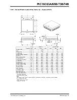
Page 157: ...2 704 695 D Overall Length 7 59 7 49 7 32 299 295 288 E1 Molded Package Width 10 67 10 34 10 01 420 407 394 E Overall Width 0 30 0 20 0 10 012 008 004 A1 Standoff 2 39 2 31 2 24 094 091 088 A2 Molded Package Thickness 2 64 2 50 2 36 104 099 093 A Overall Height 1 27 050 p Pitch 28 28 n Number of Pins MAX NOM MIN MAX NOM MIN Dimension Limits MILLIMETERS INCHES Units 2 1 D p n B E E1 L c β 45 h φ A2...

Page 158: ... 38 0 32 0 25 015 013 010 B Lead Width 203 20 101 60 0 00 8 4 0 φ Foot Angle 0 25 0 18 0 10 010 007 004 c Lead Thickness 0 94 0 75 0 56 037 030 022 L Foot Length 10 34 10 20 10 06 407 402 396 D Overall Length 5 38 5 25 5 11 212 207 201 E1 Molded Package Width 8 10 7 85 7 59 319 309 299 E Overall Width 0 25 0 15 0 05 010 006 002 A1 Standoff 1 83 1 73 1 63 072 068 064 A2 Molded Package Thickness 1 9...

Page 159: ...94 2 065 2 058 2 045 D Overall Length 14 22 13 84 13 46 560 545 530 E1 Molded Package Width 15 88 15 24 15 11 625 600 595 E Shoulder to Shoulder Width 0 38 015 A1 Base to Seating Plane 4 06 3 81 3 56 160 150 140 A2 Molded Package Thickness 4 83 4 45 4 06 190 175 160 A Top to Seating Plane 2 54 100 p Pitch 40 40 n Number of Pins MAX NOM MIN MAX NOM MIN Dimension Limits MILLIMETERS INCHES Units A2 1...

Page 160: ... 3 56 3 43 145 140 135 L Tip to Seating Plane 52 32 52 07 51 82 2 060 2 050 2 040 D Overall Length 13 36 13 21 13 06 526 520 514 E1 Ceramic Pkg Width 15 88 15 24 15 11 625 600 595 E Shoulder to Shoulder Width 1 52 1 14 0 76 060 045 030 A1 Standoff 4 19 4 06 3 94 165 160 155 A2 Ceramic Package Height 5 72 5 21 4 70 225 205 185 A Top to Seating Plane 2 54 100 p Pitch 40 40 n Number of Pins MAX NOM M...

Page 161: ...Dimension Limits MIN NOM MAX MIN NOM MAX Number of Pins n 44 44 Pitch p 031 0 80 Overall Height A 039 043 047 1 00 1 10 1 20 Molded Package Thickness A2 037 039 041 0 95 1 00 1 05 Standoff A1 002 004 006 0 05 0 10 0 15 Foot Length L 018 024 030 0 45 0 60 0 75 Foot Angle φ 0 3 5 7 0 3 5 7 Overall Width E 463 472 482 11 75 12 00 12 25 Overall Length D 463 472 482 11 75 12 00 12 25 Molded Package Wid...

Page 162: ... c Lead Thickness 11 11 n1 Pins per Side 10 10 10 00 9 90 398 394 390 Molded Package Length 10 10 10 00 9 90 398 394 390 E1 Molded Package Width 13 45 13 20 12 95 530 520 510 D Overall Length 13 45 13 20 12 95 530 520 510 Overall Width 7 3 5 0 7 3 5 0 φ Foot Angle 1 03 0 88 0 73 041 035 029 L Foot Length 0 25 0 15 0 05 010 006 002 A1 Standoff 2 10 2 03 1 95 083 080 077 A2 Molded Package Thickness ...

Page 163: ...17 53 17 40 695 690 685 D Overall Length 17 65 17 53 17 40 695 690 685 E Overall Width 0 25 0 13 0 00 010 005 000 CH2 Corner Chamfer others 1 27 1 14 1 02 050 045 040 CH1 Corner Chamfer 1 0 86 0 74 0 61 034 029 024 A3 Side 1 Chamfer Height 0 51 020 A1 Standoff A2 Molded Package Thickness 4 57 4 39 4 19 180 173 165 A Overall Height 1 27 050 p Pitch 44 44 n Number of Pins MAX NOM MIN MAX NOM MIN Dim...

Page 164: ...PIC16C63A 65B 73B 74B DS30605C page 164 2000 Microchip Technology Inc NOTES ...

Page 165: ...area in Electrical Specifications Formula for calculating A D acquisition time TACQ in the A D section Brief description of instructions Removed data see PICmicroTM Mid Range MCU Family Reference Manual DS33023 for additional data USART Baud Rate Tables formulas for calculating baud rate remain C 12 00 Minor changes to text to clarify content Revised some DC specifications Included characteristic ...

Page 166: ... or electrical changes to the device oscillator specifications the user should verify that the device oscillator starts and performs as expected Adjusting the loading capacitor values and or the oscillator mode may be required No Module Differences from PIC16C63 65A 73A 74A H W S W Prog 1 CCP CCP Special Event Trigger clears Timer1 2 Compare mode drives pin correctly 3 Timers Writing to TMR1L does...

Page 167: ...data input to SCK edge 50 100 ns 73A Note 5 TB2B Last clock edge of Byte1 to the 1st clock edge of Byte2 1 5TCY 40 ns 74 TscH2diL TscL2diL Hold time of SDI data input to SCK edge 50 100 ns 75 TdoR SDO data output rise time PIC16CXX 10 25 10 25 ns PIC16LCXX 20 45 ns 78 TscR SCK output rise time Master mode PIC16CXX 10 25 10 25 ns PIC16LCXX 20 45 ns 80 TscH2doV TscL2doV SDO data output valid after S...

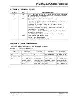
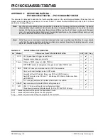
Page 168: ...hrough interrupt is added 11 Two separate timers Oscillator Start up Timer OST and Power up Timer PWRT are included for more reliable power up These tim ers are invoked selectively to avoid unneces sary delays on power up and wake up 12 PORTB has weak pull ups and interrupt on change feature 13 T0CKI pin is also a port pin RA4 now 14 FSR is made a full 8 bit register 15 In Circuit Serial Programmi...

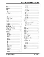
Page 169: ... In I O Port Mode 34 PORTD and PORTE as a Parallel Slave Port 37 PORTE In I O Port Mode 35 PWM 52 RA4 T0CKI Pin 29 RB3 RB0 Port Pins 31 RB7 RB4 Port Pins 31 SSP in I2 C Mode 60 SSP in SPI Mode 55 Timer0 WDT Prescaler 39 Timer2 47 USART Receive 70 USART Transmit 68 Watchdog Timer 96 BOR bit 25 89 BRGH bit 67 Brown out Reset BOR Timing Diagram 126 Buffer Full Status bit BF 56 C C bit 19 Capture Comp...

Page 170: ...truction Cycle 14 Instruction Flow Pipelining 14 Instruction Format 99 Instruction Set ADDLW 101 ADDWF 101 ANDLW 101 ANDWF 101 BCF 101 BSF 101 BTFSC 102 BTFSS 102 CALL 102 CLRF 102 CLRW 102 CLRWDT 102 COMF 103 DECF 103 DECFSZ 103 GOTO 103 INCF 103 INCFSZ 103 IORLW 104 IORWF 104 MOVF 104 MOVLW 104 MOVWF 104 NOP 104 RETFIE 105 RETLW 105 RETURN 105 RLF 105 RRF 105 SLEEP 105 SUBLW 106 SUBWF 106 SWAPF ...

Page 171: ...2 RB7 11 12 RC0 T1OSO T1CKI 11 13 RC1 T1OSI CCP2 11 13 RC2 CCP1 11 13 RC3 SCK SCL 11 13 RC4 SDI SDA 11 13 RC5 SDO 11 13 RC6 TX CK 11 13 65 76 RC7 RX DT 11 13 65 76 RD0 PSP0 13 RD1 PSP1 13 RD2 PSP2 13 RD3 PSP3 13 RD4 PSP4 13 RD5 PSP5 13 RD6 PSP6 13 RD7 PSP7 13 RE0 RD AN5 13 RE1 WR AN6 13 RE2 CS AN7 13 VDD 11 13 VSS 11 13 Pinout Descriptions PIC16C73 11 PIC16C73A 11 PIC16C74 12 PIC16C74A 12 PIC16C76...

Page 172: ...55 Serial Data In 55 Serial Data Out 55 Slave Mode Timing 59 Slave Mode Timing Diagram 58 Slave Select 55 SSPCON 57 SSPSTAT 56 SPI Clock Edge Select bit CKE 56 SPI Data Input Sample Phase Select bit SMP 56 SREN bit 66 SSP Module Overview 55 Section 55 SSPCON 57 SSPSTAT 56 SSPADD Register 18 SSPBUF Register 17 SSPCON 57 SSPCON Register 17 SSPEN 57 SSPM3 SSPM0 57 SSPOV 57 60 SSPSTAT Register 18 56 S...

Page 173: ...CS bit 43 TMR1H Register 17 TMR1L Register 17 TMR1ON bit 43 TMR2 Register 17 TMR2ON bit 47 TO bit 19 TOUTPS0 bit 47 TOUTPS1 bit 47 TOUTPS2 bit 47 TOUTPS3 bit 47 TRISA Register 18 29 TRISB Register 18 31 TRISC Register 18 33 TRISD Register 18 34 TRISE Register 18 35 36 TXSTA Register 65 U UA 56 Universal Synchronous Asynchronous Receiver Transmitter USART 65 Update Address bit UA 56 USART Asynchron...

Page 174: ...PIC16C63A 65B 73B 74B DS30605C page 174 2000 Microchip Technology Inc NOTES ...

Page 175: ...est Microchip Press Releases Technical Support Section with Frequently Asked Questions Design Tips Device Errata Job Postings Microchip Consultant Program Member Listing Links to other useful web sites related to Microchip Products Conferences for products Development Systems technical information and more Listing of seminars and events Systems Information and Upgrade Hot Line The Systems Informat...

Page 176: ...s this document meet your hardware and software development needs 3 Do you find the organization of this data sheet easy to follow If not why 4 What additions to the data sheet do you think would enhance the structure and subject 5 What deletions from the data sheet could be made without affecting the overall usefulness 6 Is there any incorrect or misleading information what and where 7 How would ...

Page 177: ... Skinny plastic dip P PDIP L PLCC SS SSOP Pattern QTP SQTP Code or Special Requirements blank otherwise Examples a PIC16C74B 04 P 301 Commercial temp PDIP package 4 MHz normal VDD limits QTP pattern 301 b PIC16LC63A 04I SO Industrial temp SOIC package 200 kHz Extended VDD limits c PIC16C65B 20I P Industrial temp PDIP package 20 MHz normal VDD limits Note 1 C CMOS LC Low Power CMOS 2 T in tape and ...

Page 178: ...PIC16C63A 65B 73B 74B DS30605C page 178 2000 Microchip Technology Inc NOTES ...

Page 179: ... 2000 Microchip Technology Inc DS30605C page 179 PIC16C63A 65B 73B 74B NOTES ...

Page 180: ...PIC16C63A 65B 73B 74B DS30605C page 180 2000 Microchip Technology Inc NOTES ...

Page 181: ... 2000 Microchip Technology Inc DS30605C page 181 PIC16C63A 65B 73B 74B NOTES ...

Page 182: ...PIC16C63A 65B 73B 74B DS30605C page 182 2000 Microchip Technology Inc NOTES ...

Page 183: ... 2000 Microchip Technology Inc DS30605C page 183 PIC16C63A 65B 73B 74B NOTES ...

Page 184: ...905 673 0699 Fax 905 673 6509 ASIA PACIFIC China Beijing Microchip Technology Beijing Office Unit 915 New China Hong Kong Manhattan Bldg No 6 Chaoyangmen Beidajie Beijing 100027 No China Tel 86 10 85282100 Fax 86 10 85282104 China Shanghai Microchip Technology Shanghai Office Room 701 Bldg B Far East International Plaza No 317 Xian Xia Road Shanghai 200051 Tel 86 21 6275 5700 Fax 86 21 6275 5060 H...

Reviews: