background image

PIC16F716

DS41206A-page 18

Preliminary

 2003 Microchip Technology Inc.

2.5

Indirect Addressing, INDF and 
FSR Registers

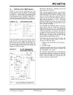
The INDF register is not a physical register. Addressing
INDF actually addresses the register whose address is
contained in the FSR register (FSR is a pointer). This is
indirect addressing.

EXAMPLE 2-1:

INDIRECT ADDRESSING

• Register file 05 contains the value 10h

• Register file 06 contains the value 0Ah

• Load the value 05 into the FSR register

• A read of the INDF register will return the value of 

10h

• Increment the value of the FSR register by one 

(FSR = 06)

• A read of the INDR register now will return the 

value of 0Ah.

Reading INDF itself indirectly (FSR = 

0

) will produce

00h. Writing to the INDF register indirectly results in a
no-operation (although Status bits may be affected).

A simple program to clear RAM locations 20h – 2Fh
using indirect addressing is shown in Example 2-2.

EXAMPLE 2-2:

HOW TO CLEAR RAM 
USING INDIRECT 
ADDRESSING 

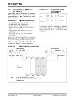
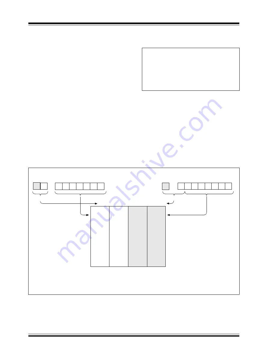
An effective 9-bit address is obtained by concatenating
the 8-bit FSR register and the IRP bit (STATUS<7>), as
shown in Figure 2-4. However, IRP is not used in the
PIC16F716.

FIGURE 2-4:

DIRECT/INDIRECT ADDRESSING

MOVLW

0x20

;initialize pointer

MOVWF

FSR

;to RAM

NEXT

CLRF

INDF

;clear RAM & FSR

INCF

FSR

;inc pointer

BTFSS

FSR,4

;all done?

GOTO

NEXT

;no, clear next

CONTINUE

:

;yes, continue

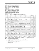
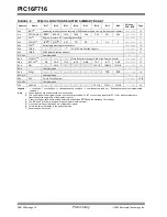
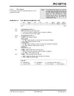
Note

1:

For register file map detail see Figure 2-2.

2:

Maintain clear for upward compatibility with future products.

3:

Not implemented.

Data
Memory

(1)

Indirect Addressing

Direct Addressing

bank select

location select

RP1: RP0

6

0

from opcode

IRP

FSR register

7

0

bank select

location select

00

01

10

11

Bank 0

Bank 1

Bank 2

Bank 3

FFh

80h

7Fh

00h

17Fh

100h

1FFh

180h

(3)

(3)

(2)

(2)

Summary of Contents for PIC16F716

Page 1: ...2003 Microchip Technology Inc Preliminary DS41206A PIC16F716 Data Sheet 8 bit Flash based Microcontroller with A D Converter and Enhanced Capture Compare PWM...

Page 2: ...2003 Microchip Technology Incorporated Printed in the U S A All Rights Reserved Printed on recycled paper Note the following details of the code protection feature on Microchip devices Microchip prod...

Page 3: ...5 25 mA Wide temperature range Industrial 40 C to 85 C Extended 40 C to 125 C Low Power Features Standby Current 100 nA 2 0V typical Operating Current 14 A 32 kHz 2 0V typical 120 A 1 MHz 2 0V typical...

Page 4: ...13 12 8 9 11 10 18 pin PDIP SOIC MCLR VPP RA3 AN3 VREF RB2 T1OSI RB3 CCP1 P1A RB4 ECCPAS0 RB5 P1B RA1 AN1 VDD OSC2 CLKOUT VSS RA2 AN2 RA4 T0CKI RB0 INT ECCPAS2 RB1 T1OSO T1CKI RA0 AN0 OSC1 CLKIN RB7 P...

Page 5: ...endix B Conversion Considerations 113 Appendix C Migration from Base line to MID RANGE Devices 114 On Line Support 115 Systems Information and Upgrade Hot Line 115 Reader Response 116 Index 117 Produc...

Page 6: ...PIC16F716 DS41206A page 4 Preliminary 2003 Microchip Technology Inc NOTES...

Page 7: ...dules Figure 1 1 is the block diagram for the PIC16F716 device The pinouts are listed in Table 1 1 FIGURE 1 1 PIC16F716 BLOCK DIAGRAM Flash Program Memory 13 Data Bus 8 14 Program Bus Instruction reg...

Page 8: ...rupt ECCPAS2 ST ECCP Auto Shutdown pin RB1 T1OSO T1CKI RB1 TTL CMOS Bidirectional I O Programmable weak pull up T1OSO XTAL Timer1 oscillator output Connects to crystal in Oscillator mode T1CKI ST Time...

Page 9: ...mory Organization The data memory is partitioned into multiple banks which contain the General Purpose Registers GPR and the Special Function Registers SFR Bits RP1 and RP0 of the Status register are...

Page 10: ...1 80h 01h TMR0 OPTION_REG 81h 02h PCL PCL 82h 03h STATUS STATUS 83h 04h FSR FSR 84h 05h PORTA TRISA 85h 06h PORTB TRISB 86h 07h 87h 08h 88h 09h 89h 0Ah PCLATH PCLATH 8Ah 0Bh INTCON INTCON 8Bh 0Ch PIR...

Page 11: ...ADIF CCP1IF TMR2IF TMR1IF 0 0000 15 0Dh Unimplemented 0Eh TMR1L Holding register for the Least Significant Byte of the 16 bit TMR1 register xxxx xxxx 29 0Fh TMR1H Holding register for the Most Signif...

Page 12: ...unter 0 0000 17 8Bh INTCON 1 GIE PEIE T0IE INTE RBIE T0IF INTF RBIF 0000 000x 13 8Ch PIE1 ADIE CCP1IE TMR2IE TMR1IE 0 000 14 8Dh Unimplemented 8Eh PCON POR BOR qq 16 8Fh 91h Unimplemented 92h PR2 Time...

Page 13: ...tively in sub traction See the SUBLW and SUBWF instructions for examples R W 0 R W 0 R W 0 R 1 R 1 R W x R W x R W x IRP 1 RP1 1 RP0 TO PD Z DC C bit 7 bit 0 bit 7 IRP Register Bank Select bit used fo...

Page 14: ...PORTB weak pull ups are determined by alternate function or TRISBn bit value bit 6 INTEDG Interrupt Edge Select bit 1 Interrupt on rising edge of RB0 INT pin 0 Interrupt on falling edge of RB0 INT pi...

Page 15: ...es all un masked peripheral interrupts 0 Disables all peripheral interrupts bit 5 T0IE TMR0 Overflow Interrupt Enable bit 1 Enables the TMR0 interrupt 0 Disables the TMR0 interrupt bit 4 INTE RB0 INT...

Page 16: ...verter Interrupt Enable bit 1 Enables the A D interrupt 0 Disables the A D interrupt bit 5 3 Unimplemented Read as 0 bit 2 CCP1IE CCP1 Interrupt Enable bit 1 Enables the CCP1 interrupt 0 Disables the...

Page 17: ...An A D conversion completed must be cleared in software 0 The A D conversion is not complete bit 5 3 Unimplemented Read as 0 bit 2 CCP1IF CCP1 Interrupt Flag bit Capture Mode 1 A TMR1 register captur...

Page 18: ...set by the user and checked on subsequent resets to see if it is clear indicating that another Brown out has occurred If the BOREN configuration bit is clear BOR is unknown on Power on Reset U 0 U 0 U...

Page 19: ...is register contains the PC 12 8 bits and is not directly readable or writable All updates to the PCH register go through the PCLATH register 2 3 1 MODIFYING PCL Executing any instruction with the PCL...

Page 20: ...eration although Status bits may be affected A simple program to clear RAM locations 20h 2Fh using indirect addressing is shown in Example 2 2 EXAMPLE 2 2 HOW TO CLEAR RAM USING INDIRECT ADDRESSING An...

Page 21: ...is multiplexed with the Timer0 module clock input to become the RA4 T0CKI pin The RA4 T0CKI pin is a Schmitt Trigger input and an open drain output All other RA port pins have TTL input levels and fu...

Page 22: ...utput or analog input RA2 AN2 bit 2 TTL Input output or analog input RA3 AN3 VREF bit 3 TTL Input output or analog input or VREF RA4 T0CKI bit 4 ST Input output or external clock input for Timer0 Outp...

Page 23: ...settings Four of PORTB s pins RB7 RB4 have an interrupt on change feature Only pins configured as inputs can cause this interrupt to occur i e any RB7 RB4 pin configured as an output is excluded from...

Page 24: ...imer1 clock input P VDD weak pull up RBPU 1 T1OSCEN VSS VDD Note 1 To enable weak pull ups set the appropriate TRIS bit s and clear the RBPU bit OPTION_REG 7 RD TRISB D Q EN TMR1 oscillator ST Buffer...

Page 25: ...ble weak pull ups set the appropriate TRIS bit s and clear the RBPU bit OPTION_REG 7 PWMA P1A CCP1 Compare Output PWMA P1A Auto shutdown tri state RD TRIS D Q EN Schmitt Trigger Buffer CCP Capture inp...

Page 26: ...propriate TRIS bit s and clear the RBPU bit OPTION_REG 7 VSS VDD RB5 P1B 0 1 Q PWMB P1B Enable PWMB P1B Data out PWMB P1B Auto shutdown tri state Data Latch From other RBPU 1 P VDD Q D CK Q D CK Q D E...

Page 27: ...le weak pull up ECCP auto shutdown input RB5 P1B bit 5 TTL Input output pin with interrupt on change Internal software programmable weak pull up PWM B output RB6 P1C bit 6 TTL ST 2 Input output pin wi...

Page 28: ...it 6 Bit 5 Bit 4 Bit 3 Bit 2 Bit 1 Bit 0 Value on POR BOR Value on all other Resets 06h PORTB RB7 RB6 RB5 RB4 RB3 RB2 RB1 RB0 xxxx xxxx uuuu uuuu 86h TRISB PORTB Data Direction Register 1111 1111 1111...

Page 29: ...in the PICmicro Mid Range Reference Manual DS33023 4 2 Prescaler An 8 bit counter is available as a prescaler for the Timer0 module or as a postscaler for the Watchdog Timer respectively Figure 4 2 F...

Page 30: ...ction sequence shown in the PICmicro Mid Range Reference Manual DS33023 must be executed when changing the prescaler assignment from Timer0 to the WDT This sequence must be followed even if the WDT is...

Page 31: ...t is the TRISB 2 1 value is ignored Timer1 also has an internal Reset input This Reset can be generated by the ECCP module Section 7 0 Enhanced Capture Compare PWM ECCP Module REGISTER 5 1 T1CON TIMER...

Page 32: ...eration the CCPR1H CCPR1L register pair effectively becomes the period register for Timer1 TABLE 5 1 REGISTERS ASSOCIATED WITH TIMER1 AS A TIMER COUNTER TMR1H TMR1L T1OSC T1SYNC TMR1CS T1CKPS1 T1CKPS0...

Page 33: ...TER 6 1 T2CON TIMER2 CONTROL REGISTER ADDRESS 12h U 0 R W 0 R W 0 R W 0 R W 0 R W 0 R W 0 R W 0 TOUTPS3 TOUTPS2 TOUTPS1 TOUTPS0 TMR2ON T2CKPS1 T2CKPS0 bit 7 bit 0 bit 7 Unimplemented Read as 0 bit 6 3...

Page 34: ...rite to the TMR2 register A write to the T2CON register Any device Reset Power on Reset MCLR Reset Watchdog Timer Reset or Brown out Reset TMR2 is not cleared when T2CON is written 6 2 Timer2 Interrup...

Page 35: ......

Page 36: ...eans that any Reset will clear the prescaler counter Switching from one capture prescaler to another may generate an interrupt Also the prescaler counter will not be cleared therefore the first captur...

Page 37: ...ot the PORTB I O data latch Note The special event trigger from the ECCP module will not set interrupt flag bit TMR1IF PIR1 0 CCPR1H CCPR1L TMR1H TMR1L Comparator Q S R Output Logic Special Event Trig...

Page 38: ...following formula EQUATION 7 1 PWM frequency is defined as 1 PWM period When TMR2 is equal to PR2 the following three events occur on the next increment cycle TMR2 is cleared The CCP1 pin is set exce...

Page 39: ...y writing to the CCPR1L register and CCP1CON 5 4 bits 3 Make the CCP1 pin an output by clearing the TRISB 3 bit 4 Set the TMR2 prescale value and enable Timer2 by writing to T2CON 5 Configure the CCP1...

Page 40: ...mer resets instead of starting immediately This means that enhanced PWM waveforms do not exactly match the standard PWM waveforms but are instead offset by one full instruction cycle 4 TOSC As before...

Page 41: ...Single Output Half Bridge Full Bridge Forward Full Bridge Reverse Delay 1 Delay 1 0 Period 00 10 01 11 SIGNAL PR2 1 CCP1CON 7 6 P1A Modulated P1A Modulated P1B Modulated P1A Active P1B Inactive P1C In...

Page 42: ...ACTIVE HIGH P1B P1D ACTIVE LOW 0 Period 00 10 01 11 SIGNAL PR2 1 CCP1CON 7 6 P1A Modulated P1A Modulated P1B Modulated P1A Active P1B Inactive P1C Inactive P1D Modulated P1A Inactive P1B Modulated P1C...

Page 43: ...Active P1B Inactive P1C Inactive P1D Modulated P1A Inactive P1B Modulated P1C Active P1D Inactive Duty Cycle Single Output Half Bridge Full Bridge Forward Full Bridge Reverse Delay 1 Delay 1 Relation...

Page 44: ...before the output is driven active If the value is greater than the duty cycle the corresponding output remains inactive during the entire cycle See Section 7 4 4 Programmable Dead Band Delay for mor...

Page 45: ...PWM period the modulated outputs P1B and P1D are placed in their inactive state while the unmodulated outputs P1A and P1C are switched to drive in the opposite direction This occurs in a time interva...

Page 46: ...at can drive the switches off faster than they can drive them on Other options to prevent shoot through current may exist FIGURE 7 13 PWM DIRECTION CHANGE FIGURE 7 14 PWM DIRECTION CHANGE AT NEAR 100...

Page 47: ...r any of the enhanced PWM modes the active output pins may be configured for auto shutdown Auto shutdown immediately places the enhanced PWM output pins into a defined shutdown state when a shutdown e...

Page 48: ...t 0 Bit is cleared x Bit is unknown R W 0 R W 0 U 0 R W 0 R W 0 R W 0 R W 0 R W 0 ECCPASE ECCPAS2 ECCPAS0 PSSAC1 PSSAC0 PSSBD1 PSSBD0 bit 7 bit 0 bit 7 ECCPASE ECCP Auto Shutdown Event Status bit 1 A...

Page 49: ...the I O pins with the proper signal levels or activates the PWM output s The CCP1M1 CCP1M0 bits CCP1CON 1 0 allow the user to choose whether the PWM output signals are active high or active low for e...

Page 50: ...r a new PWM cycle has started Wait until TMR2 overflows TMR2IF bit is set Enable the CCP1 P1A P1B P1C and or P1D pin outputs by clearing the respective TRISB bits Clear the ECCPASE bit ECCPAS 7 See th...

Page 51: ...the A D module to be turned off and any conversion is aborted The ADCON0 register shown in Register 8 1 controls the operation of the A D module The ADCON1 register shown in Register 8 2 configures t...

Page 52: ...1 Configure the A D module Configure analog pins voltage reference and digital I O ADCON1 Select A D input channel ADCON0 Select A D conversion clock ADCON0 Turn on A D module ADCON0 2 Configure A D i...

Page 53: ...efore the conversion can be started To calculate the minimum acquisition time TACQ see the PICmicro Mid Range Reference Manual DS33023 This equation calculates the acquisition time to within 1 2 LSb e...

Page 54: ...the CHS2 CHS0 bits and the TRIS bits TABLE 8 1 TAD vs DEVICE OPERATING FREQUENCIES Note 1 When reading the port register all pins configured as analog input channels will read as cleared a low level P...

Page 55: ...sion If the A D module is not enabled ADON is cleared then the special event trigger will be ignored by the A D module but will still reset the Timer1 counter TABLE 8 2 SUMMARY OF A D REGISTERS Note T...

Page 56: ......

Page 57: ...es a fixed delay on power up only and is designed to keep the part in Reset while the power supply stabilizes With these two timers on chip most applications need no external Reset circuitry Sleep mod...

Page 58: ...5V bit 6 BOREN Brown out Reset Enable bit 1 1 BOR enabled 0 BOR disabled bit 5 4 Unimplemented Read as 1 bit 3 PWRTE Power up Timer Enable bit 1 1 PWRT disabled 0 PWRT enabled bit 2 WDTE Watchdog Time...

Page 59: ...2 for recommended values of C1 and C2 2 A series resistor RS may be required 3 RF varies with the crystal chosen C1 1 C2 1 XTAL OSC2 OSC1 RF 3 Sleep To logic PIC16F716 RS 2 internal OSC1 OSC2 Open Cl...

Page 60: ......

Page 61: ...try A configuration bit BOREN can disable if clear pro grammed or enable if set the Brown out Reset circuitry The BORV configuration bit selects the programmable Brown out Reset threshold voltage VBOR...

Page 62: ...DT Module VDD rise detect OST PWRT On chip RC OSC WDT Time out Power on Reset OST 10 bit Ripple counter PWRT Chip_Reset 10 bit Ripple counter Reset Enable OST Sleep Note 1 This is a separate oscillato...

Page 63: ...xpensive albeit less accurate Transistor Q1 turns off when VDD is below a certain level such that 2 Internal Brown out Reset should be disabled when using this circuit 3 Resistors should be adjusted f...

Page 64: ...Register PCON The Power Control Status Register PCON has two bits Bit 0 is the Brown out Reset Status bit BOR If the BOREN configuration bit is set BOR is 1 on Power on Reset and reset to 0 when a Br...

Page 65: ...N 1 000h 0001 1xxx 01 MCLR Reset during normal operation 000h 000u uuuu uu MCLR Reset during Sleep 000h 0001 0uuu uu WDT Reset 000h 0000 1uuu uu WDT Wake up PC 1 uuu0 0uuu uu Brown out Reset 000h 0001...

Page 66: ...uuuu uuuu uuuu CCPR1H xxxx xxxx uuuu uuuu uuuu uuuu CCP1CON 0000 0000 0000 0000 uuuu uuuu PWM1CON 0000 0000 0000 0000 uuuu uuuu ECCPAS 00 0 0000 00 0 0000 u uu uuuu ADRES xxxx xxxx uuuu uuuu uuuu uuuu...

Page 67: ...UT SEQUENCE ON POWER UP MCLR NOT TIED TO VDD CASE 1 FIGURE 9 12 TIME OUT SEQUENCE ON POWER UP MCLR NOT TIED TO VDD CASE 2 TPWRT TOST VDD MCLR INTERNAL POR PWRT TIME OUT OST TIME OUT INTERNAL RESET TPW...

Page 68: ...special function registers PIR1 and PIR2 The corresponding interrupt enable bits are contained in special function registers PIE1 and PIE2 and the peripheral interrupt enable bit is contained in spec...

Page 69: ...saved on the stack Typically users may wish to save key registers during an interrupt i e W register and Status register This will have to be implemented in firmware Example 9 1 stores and restores th...

Page 70: ...l Specifications section under TWDT parame ter 31 Values for the WDT prescaler actually a postscaler but shared with the Timer0 prescaler may be assigned using the OPTION_REG register FIGURE 9 14 WATC...

Page 71: ...er 2 ECCP capture mode interrupt 3 ADC running in ADRC mode Other peripherals cannot generate interrupts since during Sleep no on chip clocks are present When the SLEEP instruction is being executed t...

Page 72: ...programmed while in the end application circuit This is simply done with two lines for clock and data and three other lines for power ground and the programming voltage This allows customers to manuf...

Page 73: ...equency of 4 MHz the normal instruction execution time is 1 s If a conditional test is true or the program counter is changed as a result of an instruction the instruction execution time is 2 s Table...

Page 74: ...Bit Set f Bit Test f Skip if Clear Bit Test f Skip if Set 1 1 1 2 1 2 01 01 01 01 00bb 01bb 10bb 11bb bfff bfff bfff bfff ffff ffff ffff ffff 1 2 1 2 3 3 LITERAL AND CONTROL OPERATIONS ADDLW ANDLW CAL...

Page 75: ...is 1 the result is stored back in register f Words 1 Cycles 1 Example ADDWF REG1 0 Before Instruction W 0x17 REG1 0xC2 After Instruction W 0xD9 REG1 0xC2 Z 0 C 0 DC 0 ANDLW AND Literal with W Syntax l...

Page 76: ...er f is set Words 1 Cycles 1 Example BSF REG1 7 Before Instruction REG1 0x0A After Instruction REG1 0x8A BTFSC Bit Test f Skip if Clear Syntax label BTFSC f b Operands 0 f 127 0 b 7 Operation skip if...

Page 77: ...if FLAG 1 1 PC address TRUE CALL Call Subroutine Syntax label CALL k Operands 0 k 2047 Operation PC 1 TOS k PC 10 0 PCLATH 4 3 PC 12 11 Status Affected None Encoding 10 0kkk kkkk kkkk Description Call...

Page 78: ...CLRWDT Before Instruction WDT counter After Instruction WDT counter 0x00 WDT prescaler 0 TO 1 PD 1 COMF Complement f Syntax label COMF f d Operands 0 f 127 d 0 1 Operation f dest Status Affected Z Enc...

Page 79: ...ded A NOP is executed instead making it a two cycle instruction Words 1 Cycles 1 2 Example HERE DECFSZ REG1 1 GOTO LOOP CONTINUE Before Instruction PC address HERE After Instruction REG1 REG1 1 if REG...

Page 80: ...0 Z 1 INCFSZ Increment f Skip if 0 Syntax label INCFSZ f d Operands 0 f 127 d 0 1 Operation f 1 dest skip if result 0 Status Affected None Encoding 00 1111 dfff ffff Description The contents of regist...

Page 81: ...ult is placed back in register f Words 1 Cycles 1 Example IORWF REG1 0 Before Instruction REG1 0x13 W 0x91 After Instruction REG1 0x13 W 0x93 Z 1 MOVLW Move Literal to W Syntax label MOVLW k Operands...

Page 82: ...one Encoding 00 0000 0110 0010 Description The contents of the W register are loaded in the OPTION register This instruction is supported for code compatibility with PIC16C5X products Since OPTION is...

Page 83: ...Return from Subroutine Syntax label RETURN Operands None Operation TOS PC Status Affected None Encoding 00 0000 0000 1000 Description Return from subroutine The stack is POPed and the top of the stac...

Page 84: ...PD Status Affected TO PD Encoding 00 0000 0110 0011 Description The power down Status bit PD is cleared Time out Status bit TO is set Watchdog Timer and its prescaler are cleared The processor is put...

Page 85: ...W 2 C 0 result is negative Z DC 0 SWAPF Swap Nibbles in f Syntax label SWAPF f d Operands 0 f 127 d 0 1 Operation f 3 0 dest 7 4 f 7 4 dest 3 0 Status Affected None Encoding 00 1110 dfff ffff Descrip...

Page 86: ...register Words 1 Cycles 1 Example XORLW 0xAF Before Instruction W 0xB5 After Instruction W 0x1A XORWF Exclusive OR W with f Syntax label XORWF f d Operands 0 f 127 d 0 1 Operation W XOR f dest Status...

Page 87: ...s An interface to debugging tools simulator programmer sold separately emulator sold separately in circuit debugger sold separately A full featured editor with color coded context A multiple project m...

Page 88: ......

Page 89: ...system has been designed as a real time emulation system with advanced features that are typically found on more expensive development tools The PC platform and Microsoft Windows 32 bit operating syst...

Page 90: ...demonstration board to test firmware A prototype area extends the circuitry for additional application components Some of the features include an RS 232 interface a 2 x 16 LCD display a piezo speaker...

Page 91: ...ple Windows GUI The PICkit 1 Starter Kit includes the user s guide on CD ROM PICkit 1 tutorial software and code for vari ous applications Also included are MPLAB IDE Inte grated Development Environme...

Page 92: ...PIC16F716 DS41206A page 90 Preliminary 2003 Microchip Technology Inc NOTES...

Page 93: ...nt sunk by any I O pin 25 mA Maximum output current sourced by any I O pin 25 mA Maximum current sunk by PORTA and PORTB combined 200 mA Maximum current sourced by PORTA and PORTB combined 200 mA Note...

Page 94: ...E FREQUENCY GRAPH 85 C TA 125 C 1 6 0 2 5 4 0 3 0 0 3 5 4 5 5 0 5 5 4 10 Frequency MHz VDD 20 Volts 25 2 0 Note 1 The shaded region indicates the permissible combinations of voltage and frequency 6 0...

Page 95: ...Start Voltage to ensure internal Power on Reset signal Vss V See section on Power on Reset for details D004 D004A SVDD VDD Rise Rate to ensure internal Power on Reset signal 0 05 TBD V ms PWRT enabled...

Page 96: ...45 TBD A 5 0 D025 1 8 TBD A 2 0 T1OSC Current 2 6 TBD A 3 0 3 0 TBD A 5 0 D010 IDD Supply Current 14 17 A 2 0 FOSC 32 kHz LP Oscillator mode 23 28 A 3 0 45 60 A 5 0 D011 120 160 A 2 0 FOSC 1 MHz XT O...

Page 97: ...BOR Current 45 TBD A 5 0 D025E 2 6 TBD A 3 0 T1OSC Current 3 0 TBD A 5 0 D010E IDD Supply Current 21 TBD A 3 0 FOSC 32 kHz LP Oscillator mode 38 TBD A 5 0 D011E 182 TBD A 3 0 FOSC 1 MHz XT Oscillator...

Page 98: ...at high impedance Vss VPIN VDD Pin configured as analog input D061 MCLR RA4 T0CKI 5 A Vss VPIN VDD D063 OSC1 CLKIN 5 A Vss VPIN VDD XT HS and LP osc modes D070 IPURB PORTB weak pull up current 50 250...

Page 99: ...yp Max Units Conditions These parameters are characterized but not tested Data in Type column is at 5V 25 C unless otherwise stated These parameters are for design guidance only and are not tested Not...

Page 100: ...ND SPECIFICATIONS FIGURE 12 4 EXTERNAL CLOCK TIMING AC CHARACTERISTICS Standard Operating Conditions unless otherwise stated Operating temperature 40 C TA 85 C for industrial 40 C TA 125 C for extende...

Page 101: ...llator 2 5 s LP oscillator 15 ns HS oscillator 4 TosR TosF External Clock in OSC1 Rise or Fall Time 25 ns XT oscillator 50 ns LP oscillator 15 ns HS oscillator These parameters are characterized but n...

Page 102: ...invalid I O in hold time Standard 100 ns 18A Extended LC 200 ns 19 TIOV2OSH Port input valid to OSC1 I O in setup time 0 ns 20 TIOR Port output rise time Standard 10 40 ns 20A Extended LC 80 ns 21 TI...

Page 103: ...No Prescaler TBD TBD TBD ms VDD 5V 85 C to 125 C 32 TOST Oscillation Start up Timer Period 1024 TOSC TOSC OSC1 period 33 TPWRT Power up Timer Period 28 72 132 ms VDD 5V 40 C to 85 C TBD TBD TBD ms VD...

Page 104: ...so meet parameter 47 Synchronous Prescaler 2 4 8 Standard 15 ns Asynchronous Standard 30 ns 46 Tt1L T1CKI Low Time Synchronous Prescaler 1 0 5TCY 20 ns Must also meet parameter 47 Synchronous Prescale...

Page 105: ...Prescaler 0 5TCY 20 ns With Prescaler Standard 10 ns 52 TccP CCP1 input period 3TCY 40 N ns N prescale value 1 4 or 16 53 TccR CCP1 output rise time Standard 10 40 ns 53A Extended 80 ns 54 TccF CCP1 o...

Page 106: ...age VSS 0 3 VREF 0 3 V A30 ZAIN Recommended impedance of analog voltage source 10 0 k A40 IAD A D conversion current VDD Standard 180 A Average current consumption when A D is on 1 A50 IREF VREF input...

Page 107: ...GO Q4 to A D clock start TOSC 2 If the A D clock source is selected as RC a time of TCY is added before the A D clock starts This allows the SLEEP instruction to be executed 135 TSWC Switching from co...

Page 108: ...PIC16F716 DS41206A page 106 Preliminary 2003 Microchip Technology Inc NOTES...

Page 109: ...i e outside specified VDD range This is for information only and devices will operate properly only within the specified range The data presented in this section is a statistical summary of data coll...

Page 110: ...PIC16F716 DS41206A page 108 Preliminary 2003 Microchip Technology Inc NOTES...

Page 111: ...YY Year code last 2 digits of calendar year WW Week code week of January 1 is week 01 NNN Alphanumeric traceability code Note In the event the full Microchip part number cannot be marked on one line i...

Page 112: ...61 905 898 890 D Overall Length 6 60 6 35 6 10 260 250 240 E1 Molded Package Width 8 26 7 94 7 62 325 313 300 E Shoulder to Shoulder Width 0 38 015 A1 Base to Seating Plane 3 68 3 30 2 92 145 130 115...

Page 113: ...446 D Overall Length 7 59 7 49 7 39 299 295 291 E1 Molded Package Width 10 67 10 34 10 01 420 407 394 E Overall Width 0 30 0 20 0 10 012 008 004 A1 Standoff 2 39 2 31 2 24 094 091 088 A2 Molded Packag...

Page 114: ...30 mm SSOP 10 5 0 10 5 0 Mold Draft Angle Bottom 10 5 0 10 5 0 Mold Draft Angle Top 0 38 0 32 0 25 015 013 010 B Lead Width 203 20 101 60 0 00 8 4 0 Foot Angle 0 25 0 18 0 10 010 007 004 c Lead Thick...

Page 115: ...2003 Original data sheet However the device described in this data sheet are upgrades to PIC16C716 APPENDIX B CONVERSION CONSIDERATIONS This is a Flash program memory version of the PIC16C716 device...

Page 116: ...ups and interrupt on change feature 13 T0CKI pin is also a port pin RA4 now 14 FSR is made a full eight bit register 15 In circuit serial programming is made possible The user can program PIC16F716 de...

Page 117: ...ation Notes User s Guides Articles and Sample Programs A vari ety of Microchip specific business information is also available including listings of Microchip sales offices distributors and factory re...

Page 118: ...tions Manager RE Reader Response Total Pages Sent ________ From Name Company Address City State ZIP Country Telephone _______ _________ _________ Application optional Would you like a reply Y N Device...

Page 119: ...0 Timer2 32 Watchdog Timer WDT 67 BOR See Brown out Reset Brown out Detect BOD 59 Brown out Reset BOR 55 58 62 63 BOR Enable BODEN Bit 56 BOR Status BOR Bit 16 Timing Diagram 101 BSF Instruction 74 BT...

Page 120: ...IF Bit 13 T0IE Bit 13 T0IF Bit 13 Interrupt Sources 55 65 A D Conversion Complete 50 Capture Complete CCP 34 Compare Complete CCP 35 Interrupt on Change RB7 RB4 21 RB0 INT Pin External 66 TMR0 Overflo...

Page 121: ...5 58 62 63 Oscillator Start up Timer OST 55 59 POR Status POR Bit 16 Power Control PCON Register 62 Power down PD Bit 11 58 Power on Reset Circuit External 58 Power up Timer PWRT 55 59 PWRT Enable PWR...

Page 122: ...s of the CPU 55 Special Function Registers 9 Speed Operating 1 Stack 17 Status Register 9 66 C Bit 11 DC Bit 11 IRP Bit 11 PD Bit 11 58 RP1 RP0 Bits 11 TO Bit 11 58 Z Bit 11 SUBLW Instruction 82 SUBWF...

Page 123: ...from Sleep 55 68 Interrupts 62 63 MCLR Reset 63 Timing Diagram 69 WDT Reset 63 Watchdog Timer WDT 55 67 Enable WDTE Bit 56 67 Postscaler See Postscaler WDT Programming Considerations 67 RC Oscillator...

Page 124: ...PIC16F716 DS41206A page 122 Preliminary 2003 Microchip Technology Inc NOTES...
Page 125: ...age QTP pattern 301 b PIC16F716 E SO Extended temp SOIC package Note 1 T in tape and reel SOIC and SSOP packages only Data Sheets Products supported by a preliminary Data Sheet may have an errata shee...

Page 126: ...Far East International Plaza No 317 Xian Xia Road Shanghai 200051 Tel 86 21 6275 5700 Fax 86 21 6275 5060 China Shenzhen Rm 1812 18 F Building A United Plaza No 5022 Binhe Road Futian District Shenzhe...

Reviews: