2003 Microchip Technology Inc.
Preliminary
DS41206A-page 29
PIC16F716
5.0
TIMER1 MODULE
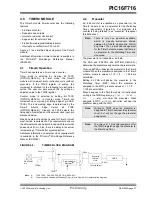
The Timer1 module timer/counter has the following
features:
• 16-bit timer/counter
(Two 8-bit registers; TMR1H and TMR1L)
• Readable and writable (Both registers)
• Internal or external clock select
• Interrupt on overflow from FFFFh to 0000h
• Reset from ECCP module trigger
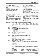
Timer1 has a control register, shown in Register 5-1.
Timer1 can be enabled/disabled by setting/clearing
control bit TMR1ON (T1CON<0>).
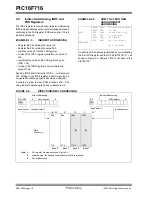
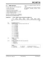
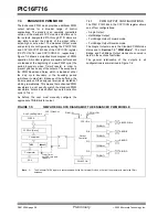
Figure 5-1 is a simplified block diagram of the Timer1
module.
Additional information on timer modules is available in
the PICmicro
®
Mid-Range Reference Manual,
(DS33023).
5.1
Timer1 Operation
Timer1 can operate in one of these modes:
• As a timer
• As a synchronous counter
• As an asynchronous counter
The operating mode is determined by the clock select
bit, TMR1CS (T1CON<1>).
In Timer mode, Timer1 increments every instruction
cycle. In Counter mode, it increments on every rising
edge of the external clock input.
When the Timer1 oscillator is enabled (T1OSCEN is
set), the RB2/T1OSI and RB1/T1OSO/T1CKI pins
become inputs. That is, the TRISB<2:1> value is
ignored.
Timer1 also has an internal “Reset input”. This Reset
can be generated by the ECCP module
(Section 7.0 “Enhanced Capture/Compare/PWM
(ECCP) Module”).
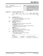
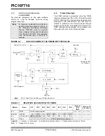
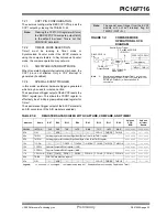
REGISTER 5-1:
T1CON: TIMER1 CONTROL REGISTER (ADDRESS: 10h)
U-0
U-0
R/W-0
R/W-0
R/W-0
R/W-0
R/W-0
R/W-0
—
—
T1CKPS1
T1CKPS0
T1OSCEN
T1SYNC TMR1CS TMR1ON
bit 7
bit 0
bit 7-6
Unimplemented: Read as '
0
'
bit 5-4
T1CKPS1:T1CKPS0: Timer1 Input Clock Prescale Select bits
11
= 1:8 Prescale value
10
= 1:4 Prescale value
01
= 1:2 Prescale value
00
= 1:1 Prescale value
bit 3
T1OSCEN: Timer1 Oscillator Enable Control bit
1
= Oscillator is enabled
0
= Oscillator is shut off
(1)
bit 2
T1SYNC: Timer1 External Clock Input Synchronization Control bit
TMR1CS =
1
1
= Do not synchronize external clock input
0
= Synchronize external clock input
TMR1CS =
0
This bit is ignored. Timer1 uses the internal clock when TMR1CS =
0
.
bit 1
TMR1CS: Timer1 Clock Source Select bit
1
= External clock from pin RB1/T1OSO/T1CKI (on the rising edge after the first falling edge)
0
= Internal clock (F
OSC
/4)
bit 0
TMR1ON: Timer1 On bit
1
= Enables Timer1
0
= Stops Timer1
Note 1:
The oscillator inverter and feedback resistor are turned off to eliminate power drain.
Legend:
R = Readable bit
W = Writable bit
U = Unimplemented bit, read as ‘
0
’
-n = Value at POR
‘1’ = Bit is set
‘0’ = Bit is cleared
x = Bit is unknown
Summary of Contents for PIC16F716
Page 6: ...PIC16F716 DS41206A page 4 Preliminary 2003 Microchip Technology Inc NOTES...
Page 35: ......
Page 56: ......
Page 60: ......
Page 88: ......
Page 92: ...PIC16F716 DS41206A page 90 Preliminary 2003 Microchip Technology Inc NOTES...
Page 108: ...PIC16F716 DS41206A page 106 Preliminary 2003 Microchip Technology Inc NOTES...
Page 110: ...PIC16F716 DS41206A page 108 Preliminary 2003 Microchip Technology Inc NOTES...
Page 124: ...PIC16F716 DS41206A page 122 Preliminary 2003 Microchip Technology Inc NOTES...

