2003 Microchip Technology Inc.
DS39582B-page 135
PIC16F87XA
12.0
COMPARATOR MODULE
The comparator module contains two analog compara-
tors. The inputs to the comparators are multiplexed
with I/O port pins RA0 through RA3, while the outputs
are multiplexed to pins RA4 and RA5. The on-chip volt-
age reference (Section 13.0 “Comparator Voltage
Reference Module”) can also be an input to the
comparators.
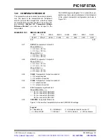
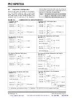
The CMCON register (Register 12-1) controls the com-
parator input and output multiplexers. A block diagram
of the various comparator configurations is shown in
Figure 12-1.
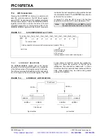
REGISTER 12-1:
CMCON REGISTER
R-0
R-0
R/W-0
R/W-0
R/W-0
R/W-1
R/W-1
R/W-1
C2OUT
C1OUT
C2INV
C1INV
CIS
CM2
CM1
CM0
bit 7
bit 0
bit 7
C2OUT: Comparator 2 Output bit
When C2INV =
0
:
1
= C2 V
IN
+ > C2 V
IN
-
0
= C2 V
IN
+ < C2 V
IN
-
When C2INV =
1
:
1
= C2 V
IN
+ < C2 V
IN
-
0
= C2 V
IN
+ > C2 V
IN
-
bit 6
C1OUT: Comparator 1 Output bit
When C1INV =
0
:
1
= C1 V
IN
+ > C1 V
IN
-
0
= C1 V
IN
+ < C1 V
IN
-
When C1INV =
1
:
1
= C1 V
IN
+ < C1 V
IN
-
0
= C1 V
IN
+ > C1 V
IN
-
bit 5
C2INV: Comparator 2 Output Inversion bit
1
= C2 output inverted
0
= C2 output not inverted
bit 4
C1INV: Comparator 1 Output Inversion bit
1
= C1 output inverted
0
= C1 output not inverted
bit 3
CIS: Comparator Input Switch bit
When CM2:CM0 =
110
:
1
= C1 V
IN
- connects to RA3/AN3
C2 V
IN
- connects to RA2/AN2
0
= C1 V
IN
- connects to RA0/AN0
C2 V
IN
- connects to RA1/AN1
bit 2
CM2:CM0: Comparator Mode bits
Figure 12-1 shows the Comparator modes and CM2:CM0 bit settings.
Legend:
R = Readable bit
W = Writable bit
U = Unimplemented bit, read as ‘0’
- n = Value at POR
‘1’ = Bit is set
‘0’ = Bit is cleared
x = Bit is unknown
http://www.xinpian.net
提供单片机解密、IC解密、芯片解密业务
010-62245566 13810019655

