2003 Microchip Technology Inc.
DS39582B-page 15
PIC16F87XA
2.0
MEMORY ORGANIZATION
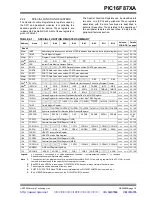
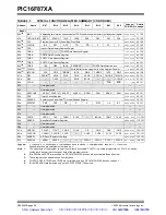
There are three memory blocks in each of the
PIC16F87XA devices. The program memory and data
memory have separate buses so that concurrent
access can occur and is detailed in this section. The
EEPROM data memory block is detailed in Section 3.0
“Data EEPROM and Flash Program Memory”.
Additional information on device memory may be found
in the PICmicro
®
Mid-Range MCU Family Reference
Manual (DS33023).
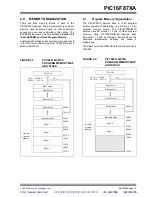
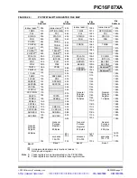
FIGURE 2-1:
PIC16F876A/877A
PROGRAM MEMORY MAP
AND STACK
2.1
Program Memory Organization
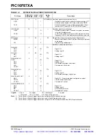
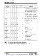
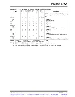
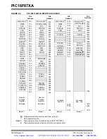
The PIC16F87XA devices have a 13-bit program
counter capable of addressing an 8K word x 14 bit
program memory space. The PIC16F876A/877A
devices have 8K words x 14 bits of Flash program
memory, while PIC16F873A/874A devices have
4K words x 14 bits. Accessing a location above the
physically implemented address will cause a
wraparound.
The Reset vector is at 0000h and the interrupt vector is
at 0004h.
FIGURE 2-2:
PIC16F873A/874A
PROGRAM MEMORY MAP
AND STACK
PC<12:0>
13
0000h
0004h
0005h
Stack Level 1
Stack Level 8
Reset Vector
Interrupt Vector
On-Chip
CALL, RETURN
RETFIE, RETLW
1FFFh
Stack Level 2
Program
Memory
Page 0
Page 1
Page 2
Page 3
07FFh
0800h
0FFFh
1000h
17FFh
1800h
PC<12:0>
13
0000h
0004h
0005h
Stack Level 1
Stack Level 8
Reset Vector
Interrupt Vector
On-Chip
CALL, RETURN
RETFIE, RETLW
1FFFh
Stack Level 2
Program
Memory
Page 0
Page 1
07FFh
0800h
0FFFh
1000h
http://www.xinpian.net
提供单片机解密、IC解密、芯片解密业务
010-62245566 13810019655

