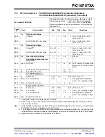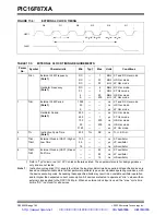
2003 Microchip Technology Inc.
DS39582B-page 187
PIC16F87XA
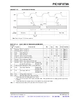
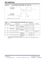
FIGURE 17-10:
PARALLEL SLAVE PORT TIMING (PIC16F874A/877A ONLY)
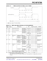
TABLE 17-8:
PARALLEL SLAVE PORT REQUIREMENTS (PIC16F874A/877A ONLY)
Note: Refer to Figure 17-3 for load conditions.
RE2/CS
RE0/RD
RE1/WR
RD7:RD0
62
63
64
65
Param
No.
Symbol
Characteristic
Min
Typ†
Max
Units
Conditions
62
T
DT
V2
WR
H
Data In Valid before WR
↑
or CS
↑
(setup time)
20
—
—
ns
63*
T
WR
H2
DT
I
WR
↑
or CS
↑
to Data–in Invalid
(hold time)
Standard(F)
20
—
—
ns
Extended(LF)
35
—
—
ns
64
T
RD
L2
DT
V
RD
↓
and CS
↓
to Data–out Valid
—
—
80
ns
65
T
RD
H2
DT
I
RD
↑
or CS
↓
to Data–out Invalid
10
—
30
ns
*
These parameters are characterized but not tested.
†
Data in “Typ” column is at 5V, 25°C unless otherwise stated. These parameters are for design guidance only and are
not tested.
http://www.xinpian.net
提供单片机解密、IC解密、芯片解密业务
010-62245566 13810019655

