2003 Microchip Technology Inc.
DS39582B-page 37
PIC16F87XA
3.6
Writing to Flash Program Memory
Flash program memory may only be written to if the
destination address is in a segment of memory that is
not write-protected, as defined in bits WRT1:WRT0 of
the device configuration word (Register 14-1). Flash
program memory must be written in four-word blocks. A
block consists of four words with sequential addresses,
with a lower boundary defined by an address, where
EEADR<1:0> =
00
. At the same time, all block writes to
program memory are done as erase and write opera-
tions. The write operation is edge-aligned and cannot
occur across boundaries.
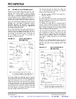
To write program data, it must first be loaded into the
buffer registers (see Figure 3-1). This is accomplished
by first writing the destination address to EEADR and
EEADRH and then writing the data to EEDATA and
EEDATH. After the address and data have been set up,
then the following sequence of events must be
executed:
1.
Set the EEPGD control bit (EECON1<7>).
2.
Write 55h, then AAh, to EECON2 (Flash
programming sequence).
3.
Set the WR control bit (EECON1<1>).
All four buffer register locations MUST be written to with
correct data. If only one, two or three words are being
written to in the block of four words, then a read from
the program memory location(s) not being written to
must be performed. This takes the data from the pro-
gram location(s) not being written and loads it into the
EEDATA and EEDATH registers. Then the sequence of
events to transfer data to the buffer registers must be
executed.
To transfer data from the buffer registers to the program
memory, the EEADR and EEADRH must point to the last
location in the four-word block (EEADR<1:0> =
11
).
Then the following sequence of events must be
executed:
1.
Set the EEPGD control bit (EECON1<7>).
2.
Write 55h, then AAh, to EECON2 (Flash
programming sequence).
3.
Set control bit WR (EECON1<1>) to begin the
write operation.
The user must follow the same specific sequence to ini-
tiate the write for each word in the program block, writ-
ing each program word in sequence (
00,01,10,11
).
When the write is performed on the last word
(EEADR<1:0> =
11
), the block of four words are
automatically erased and the contents of the buffer
registers are written into the program memory.
After the “
BSF EECON1,WR
” instruction, the processor
requires two cycles to set up the erase/write operation.
The user must place two
NOP
instructions after the WR
bit is set. Since data is being written to buffer registers,
the writing of the first three words of the block appears
to occur immediately. The processor will halt internal
operations for the typical 4 ms, only during the cycle in
which the erase takes place (i.e., the last word of the
four-word block). This is not Sleep mode as the clocks
and peripherals will continue to run. After the write
cycle, the processor will resume operation with the third
instruction after the EECON1 write instruction. If the
sequence is performed to any other location, the action
is ignored.
FIGURE 3-1:
BLOCK WRITES TO FLASH PROGRAM MEMORY
14
14
14
14
Program Memory
Buffer Register
EEADR<1:0> =
00
Buffer Register
EEADR<1:0> =
01
Buffer Register
EEADR<1:0> =
10
Buffer Register
EEADR<1:0> =
11
EEDATA
EEDATH
7
5
0 7
0
6
8
First word of block
to be written
Four words of
to Flash
automatically
after this word
is written
are transferred
Flash are erased,
then all buffers
http://www.xinpian.net
提供单片机解密、IC解密、芯片解密业务
010-62245566 13810019655

