2003 Microchip Technology Inc.
DS39582B-page 57
PIC16F87XA
6.0
TIMER1 MODULE
The Timer1 module is a 16-bit timer/counter consisting
of two 8-bit registers (TMR1H and TMR1L) which are
readable and writable. The TMR1 register pair
(TMR1H:TMR1L) increments from 0000h to FFFFh
and rolls over to 0000h. The TMR1 interrupt, if enabled,
is generated on overflow which is latched in interrupt
flag bit, TMR1IF (PIR1<0>). This interrupt can be
enabled/disabled by setting/clearing TMR1 interrupt
enable bit, TMR1IE (PIE1<0>).
Timer1 can operate in one of two modes:
• As a Timer
• As a Counter
The operating mode is determined by the clock select
bit, TMR1CS (T1CON<1>).
In Timer mode, Timer1 increments every instruction
cycle. In Counter mode, it increments on every rising
edge of the external clock input.
Timer1 can be enabled/disabled by setting/clearing
control bit, TMR1ON (T1CON<0>).
Timer1 also has an internal “Reset input”. This Reset
can be generated by either of the two CCP modules
(Section 8.0 “Capture/Compare/PWM Modules”).
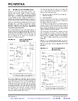
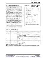
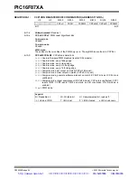
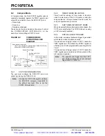
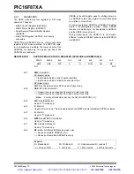
Register 6-1 shows the Timer1 Control register.
When the Timer1 oscillator is enabled (T1OSCEN is
set), the RC1/T1OSI/CCP2 and RC0/T1OSO/T1CKI
pins become inputs. That is, the TRISC<1:0> value is
ignored and these pins read as ‘
0
’.
Additional information on timer modules is available in
the PICmicro
®
Mid-Range MCU Family Reference
Manual (DS33023).
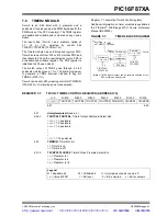
REGISTER 6-1:
T1CON: TIMER1 CONTROL REGISTER (ADDRESS 10h)
U-0
U-0
R/W-0
R/W-0
R/W-0
R/W-0
R/W-0
R/W-0
—
—
T1CKPS1 T1CKPS0
T1OSCEN
T1SYNC TMR1CS TMR1ON
bit 7
bit 0
bit 7-6
Unimplemented: Read as ‘
0
’
bit 5-4
T1CKPS1:T1CKPS0: Timer1 Input Clock Prescale Select bits
11
= 1:8 prescale value
10
= 1:4 prescale value
01
= 1:2 prescale value
00
= 1:1 prescale value
bit 3
T1OSCEN: Timer1 Oscillator Enable Control bit
1
= Oscillator is enabled
0
= Oscillator is shut-off (the oscillator inverter is turned off to eliminate power drain)
bit 2
T1SYNC: Timer1 External Clock Input Synchronization Control bit
When TMR1CS =
1
:
1
= Do not synchronize external clock input
0
= Synchronize external clock input
When TMR1CS =
0
:
This bit is ignored. Timer1 uses the internal clock when TMR1CS =
0
.
bit 1
TMR1CS: Timer1 Clock Source Select bit
1
= External clock from pin RC0/T1OSO/T1CKI (on the rising edge)
0
= Internal clock (F
OSC
/4)
bit 0
TMR1ON: Timer1 On bit
1
= Enables Timer1
0
= Stops Timer1
Legend:
R = Readable bit
W = Writable bit
U = Unimplemented bit, read as ‘0’
- n = Value at POR
‘1’ = Bit is set
‘0’ = Bit is cleared
x = Bit is unknown
http://www.xinpian.net
提供单片机解密、IC解密、芯片解密业务
010-62245566 13810019655


