2003 Microchip Technology Inc.
DS39582B-page 71
PIC16F87XA
9.0
MASTER SYNCHRONOUS
SERIAL PORT (MSSP)
MODULE
9.1
Master SSP (MSSP) Module
Overview
The Master Synchronous Serial Port (MSSP) module is
a serial interface, useful for communicating with other
peripheral or microcontroller devices. These peripheral
devices may be serial EEPROMs, shift registers,
display drivers, A/D converters, etc. The MSSP module
can operate in one of two modes:
• Serial Peripheral Interface (SPI)
• Inter-Integrated Circuit (I
2
C)
- Full Master mode
- Slave mode (with general address call)
The I
2
C interface supports the following modes in
hardware:
• Master mode
• Multi-Master mode
• Slave mode
9.2
Control Registers
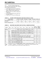
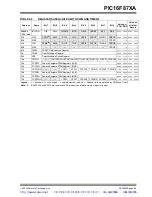
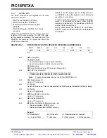
The MSSP module has three associated registers.
These include a status register (SSPSTAT) and two
control registers (SSPCON and SSPCON2). The use
of these registers and their individual configuration bits
differ significantly, depending on whether the MSSP
module is operated in SPI or I
2
C mode.
Additional details are provided under the individual
sections.
9.3
SPI Mode
The SPI mode allows 8 bits of data to be synchronously
transmitted and received simultaneously. All four
modes of SPI are supported. To accomplish
communication, typically three pins are used:
• Serial Data Out (SDO) – RC5/SDO
• Serial Data In (SDI) – RC4/SDI/SDA
• Serial Clock (SCK) – RC3/SCK/SCL
Additionally, a fourth pin may be used when in a Slave
mode of operation:
• Slave Select (SS) – RA5/AN4/SS/C2OUT
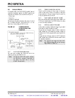
Figure 9-1 shows the block diagram of the MSSP
module when operating in SPI mode.
FIGURE 9-1:
MSSP BLOCK DIAGRAM
(SPI MODE)
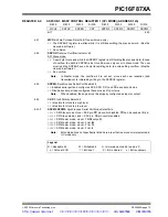
Note:
When the SPI is in Slave mode with SS pin
control enabled (SSPCON<3:0> =
0100
),
the state of the SS pin can affect the state
read back from the TRISC<5> bit. The
Peripheral OE signal from the SSP mod-
ule in PORTC controls the state that is
read back from the TRISC<5> bit (see
Section 4.3 “PORTC and the TRISC
Register” for information on PORTC). If
Read-Modify-Write instructions, such as
BSF
, are performed on the TRISC register
while the SS pin is high, this will cause the
TRISC<5> bit to be set, thus disabling the
SDO output.
Read
Write
Internal
Data Bus
SSPSR reg
SSPM3:SSPM0
bit0
Shift
Clock
SS Control
Enable
Edge
Select
Clock Select
TMR2 Output
T
OSC
Prescaler
4, 16, 64
2
Edge
Select
2
4
Data to TX/RX in SSPSR
TRIS bit
2
SMP:CKE
RC5/SDO
(
)
SSPBUF reg
RC4/SDI/SDA
RA5/AN4/
RC3/SCK/SCL
Peripheral OE
SS/C2OUT
http://www.xinpian.net
提供单片机解密、IC解密、芯片解密业务
010-62245566 13810019655


