2013 Microchip Technology Inc.
Advance Information
DS33030A-page 143
PIC24FV16KM204 FAMILY
13.0 CAPTURE/COMPARE/PWM/
TIMER MODULES (MCCP AND
SCCP)
PIC24FV16KM204 family devices include several
Capture/Compare/PWM/Timer base modules, which
provide the functionality of three different peripherals of
earlier PIC24F devices. The module can operate in one
of three major modes:
• General Purpose Timer
• Input Capture
• Output Compare/PWM
The module is provided in two different forms, distin-
guished by the number of PWM outputs that the
module can generate. Single output modules (SCCPs)
provide only one PWM output. Multiple output modules
(MCCPs) can provide up to six outputs and an
extended range of power control features, depending
on the pin count of the particular device. All other
features of the modules are identical.
The SCCP and MCCP modules can be operated only
in one of the three major modes at any time. The other
modes are not available unless the module is
reconfigured for the new mode.
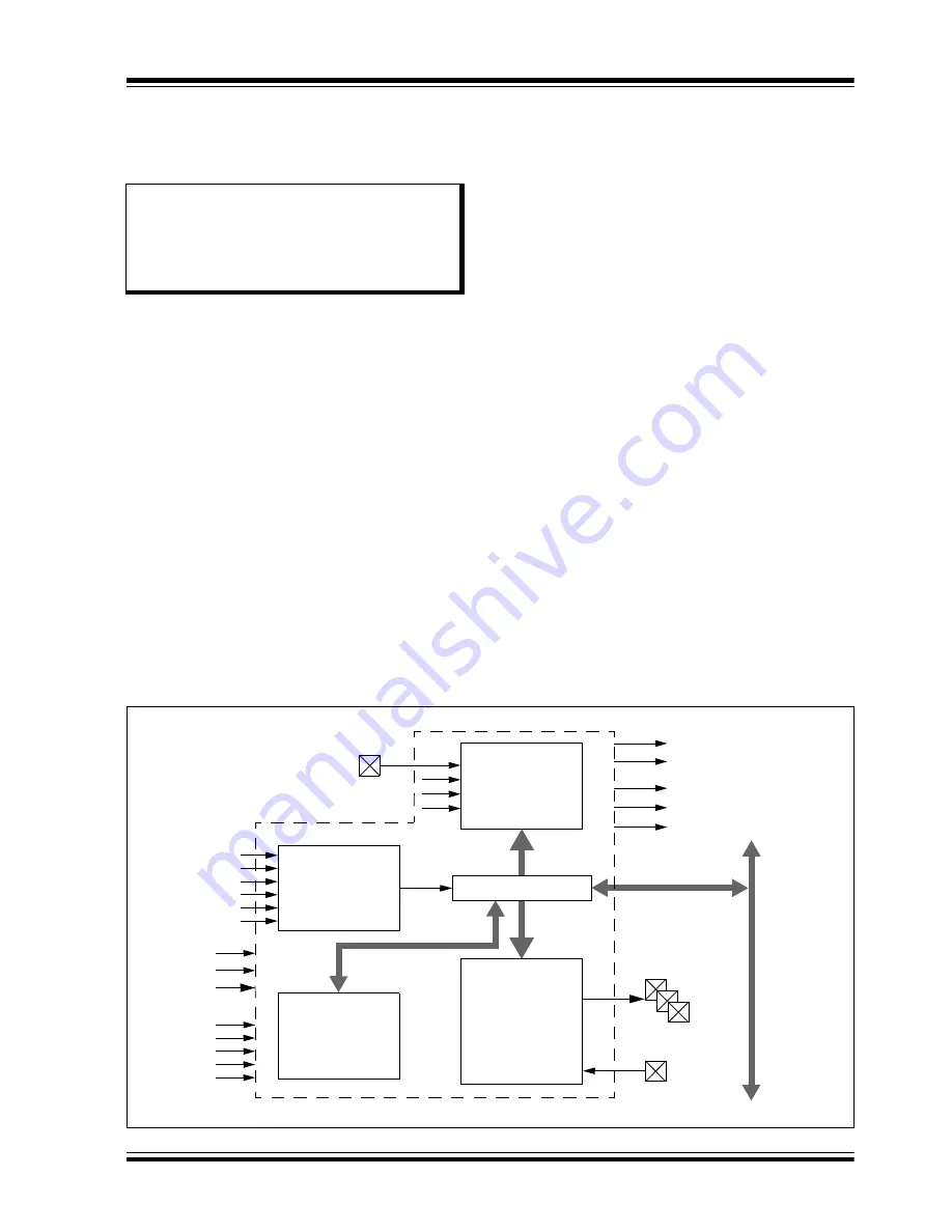
A conceptual block diagram for the module is shown in
. All three modes share a time base gener-
ator and a common Timer register pair (CCPxTMRH/L);
other shared hardware components are added as a
particular mode requires.
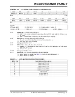
Each module has a total of seven control and status
registers:
• CCPxCON1L (
)
• CCPxCON1H (
• CCPxCON2L (
)
• CCPxCON2H (
• CCPxCON3L (
)
• CCPxCON3H (
• CCPxSTATL (
)
Each module also includes eight buffer/counter regis-
ters that serve as Timer Value registers or data holding
buffers:
• CCPxTMRH/CCPxTMRL (Timer High/Low
Counters)
• CCPxPRH/CCPxPRL (Timer Period High/Low)
• CCPxRA (Primary Output Compare Data Buffer)
• CCPxRB (Secondary Output Compare
Data Buffer)
• CCPxBUFH/CCPxBUFL (Input Capture High/Low
Buffers)
FIGURE 13-1:
MCCPx/SCCPx CONCEPTUAL BLOCK DIAGRAM TIMER CLOCK GENERATOR
Note:
This data sheet summarizes the features
of this group of PIC24F devices. It is not
intended to be a comprehensive refer-
ence source. For more information on the
MCCP/SCCP modules, refer to the
“PIC24F Family Reference Manual”
.
Clock
Sources
Input Capture
Output Compare/
PWM
T32
CCSEL
MOD<3:0>
Sync and
Gating
Sources
16/32-Bit
Auxiliary Output (to CTMU)
CCPxIF
CCTxIF
External
Compare/PWM
Output(s)
OEFA/OEFB
Timer
Sync/Trigger Out
Special Trigger (to A/D)
Capture Input
Time Base
Generator
CCPxTMRH/L
Summary of Contents for PIC24FV16KM204 FAMILY
Page 312: ...PIC24FV16KM204 FAMILY DS33030A page 312 Advance Information 2013 Microchip Technology Inc ...
Page 313: ... 2013 Microchip Technology Inc Advance Information DS33030A page 313 PIC24FV16KM204 FAMILY ...
Page 315: ... 2013 Microchip Technology Inc Advance Information DS33030A page 315 PIC24FV16KM204 FAMILY ...
Page 316: ...PIC24FV16KM204 FAMILY DS33030A page 316 Advance Information 2013 Microchip Technology Inc ...
Page 317: ... 2013 Microchip Technology Inc Advance Information DS33030A page 317 PIC24FV16KM204 FAMILY ...
Page 322: ...PIC24FV16KM204 FAMILY DS33030A page 322 Advance Information 2013 Microchip Technology Inc ...


